Multiple testing bars for testing liquid crystal display and method thereof

a liquid crystal display and multi-stage technology, applied in the field of liquid crystal display, can solve the problems of reducing the protection capability against electrostatic charges and hard to detect short-circuited elements, and achieve the effect of increasing the detection ability of visual defects and increasing reliability

Inactive Publication Date: 2012-11-13
SAMSUNG DISPLAY CO LTD
View PDF30 Cites 1 Cited by
  • Summary
  • Abstract
  • Description
  • Claims
  • Application Information

AI Technical Summary

Benefits of technology

[0015]It is an object of the present invention to provide a TFT array panel having shorting bars that are superior in detecting short-circuit defects as well as in discharging electrostatic charges.
[0016]It is another object of the present invention to provide a test method to detect short-circuit defects between adjacent data lines or adjacent gate lines and pixel defects with ease.
[0017]It is another object of the present invention to provide a test method to effectively detect some defects in a high-resolution substrate.
[0024]According to the LCDs and the manufacturing methods of the present invention, the additional gate shorting bars or the additional data shorting bars are formed and separated from the main shorting bar after the process is over. Accordingly, the LCD substrate is superior in detecting short-circuited defects of the substrate as well as in discharging the electrostatic charges.
[0026]In this test method according to the present invention, it is possible to detect short-circuited defects between adjacent pixels or adjacent wires, and the detecting ability of visual defects and the reliability are increased.

Problems solved by technology

However, if more than two gate lines or data lines, for example, the data lines D2 and D3 in FIG. 1, are short-circuited (S1), it is hard to detect the short-circuited elements since the voltage of the same magnitude and polarity is applied to the two data lines D2 and D3.
However, the protecting capability against electrostatic charges may decrease.

Method used


Image

  • Multiple testing bars for testing liquid crystal display and method thereof
  • Multiple testing bars for testing liquid crystal display and method thereof
  • Multiple testing bars for testing liquid crystal display and method thereof

Examples


first embodiment

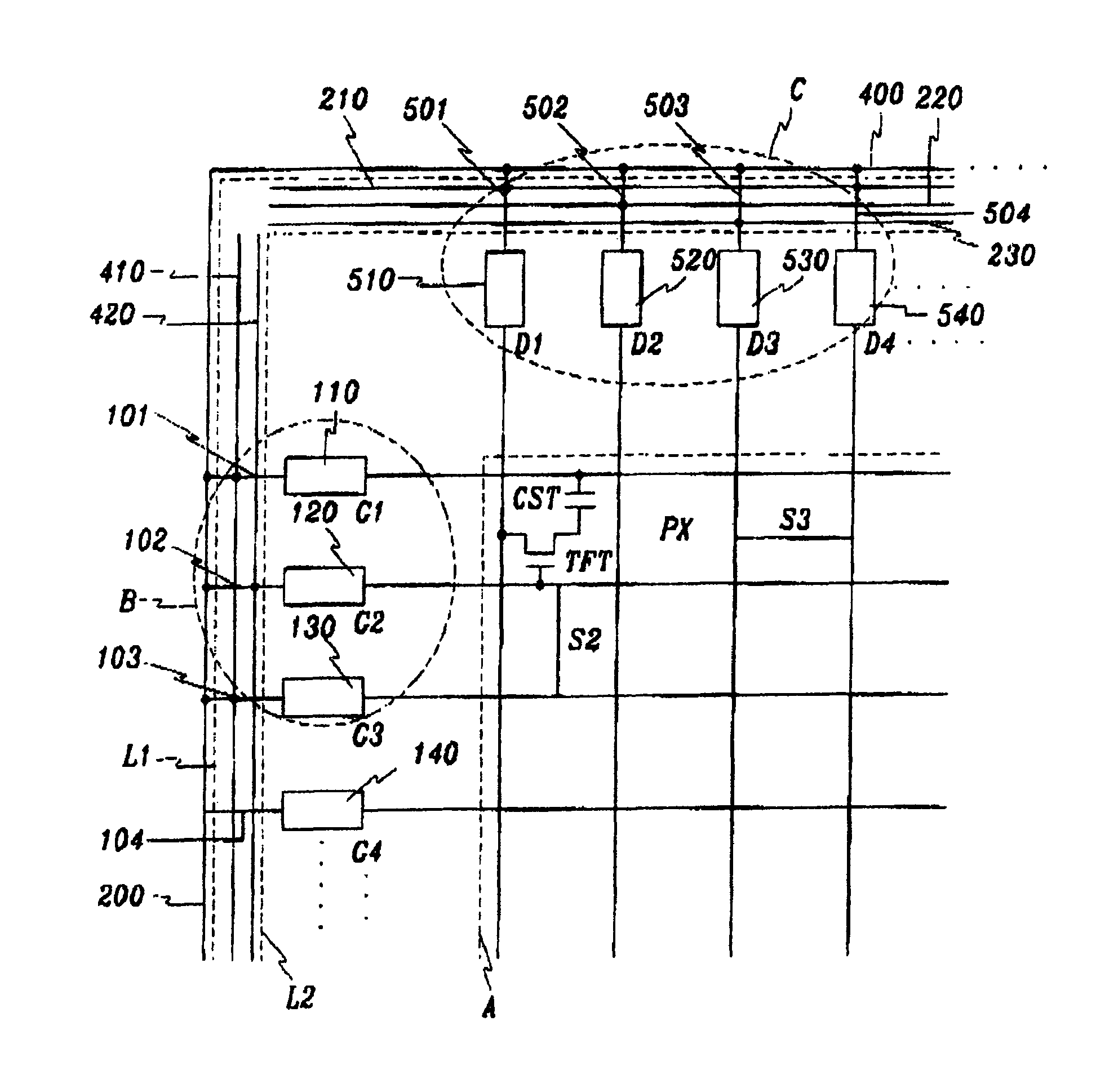
[0080]Then, a visual test method is described with references to FIGS. 13, 14 and 15A to 15C. FIG. 14 illustrates wave forms of array test signals applied to gate and data lines through the respective secondary lines and FIGS. 15A to 15C illustrate polarities of signals applied to R, G, B pixels in modes 1 to 3. As shown in FIGS. 13 and 14, signal voltages Godd and Geven are applied to a plurality of gate lines in odd rows and a plurality of gate lines in even rows. Signal voltages DR, DG and DB are respectively applied to a plurality of (3n−2)th, (3n−1)th and (3n)th data lines through the first to the fifth secondary lines 410,420,210, 220 and 230.

[0081]Then, the signal voltages are described more in detail hereinafter. Signal voltages Godd and Geven, which respectively include pulses turning on thin film transistors, are applied to odd gate lines and to even gate lines through the first and the second secondary lines 410 and 420. If the period from the moment one pulse is applied...

second embodiment

[0098]In the defect detecting method since polarities of the test signals applied to R, G and B pixel columns invert with the same period as the width of the gate pulse, the signals is not charged into the pixels sufficiently. As a result, flicker effects may occur. In addition, it is not suitable to test for visual uniformity that is usually confirmed by naked eyes, and it is difficult to detect the pixel defects under the high state or off state.

[0099]FIG. 18 shows testing wave forms according to the third embodiment to improve this problem. In FIG. 18, signals DR, DG and DB applied to R, G and B pixel columns and signals Godd and Geven applied to odd and even gate lines are mostly similar to the signals in the second embodiment. Instead, the signals applied to the R, G and B pixel columns invert with a period of two times the width of the gate pulse. Therefore, there is no difficulty in charging the R, G and B signals into the pixels, it is easy to synchronize the gate pulse and...

fourth embodiment

[0100]FIG. 19 illustrates wave forms of array test signals in which pulses are applied to the odd gate lines and to the even gate lines and the two pulses are synchronized with a half frame difference. Test signals invert with a period of twice the width of the gate pulse.

[0101]In the fourth embodiment, the gate pulse is applied later than the moment (t1, t2) when the signals DR, DG and DB applied to the R, G and B pixel columns invert. Therefore, the signals can be charged with a large initial charging value when TFTs are turned on. As a result, the charging time decreases and the signals can be charged sufficiently while the gate pulse is applied. Therefore, it is easy to test even a high resolution substrate.

[0102]As described above, in the LCD according to the present invention, since gate secondary shorting bars or data secondary shorting bars are respectively formed with more than two divided lines and separated from a gate shorting bar and a data shorting bar, the substrate ...


PUM


Abstract

A plurality of gate lines are formed on an insulating substrate in the horizontal direction, a gate shorting bar connected to the data lines is formed in the vertical direction and a gate insulating film is formed thereon. A plurality of data lines intersecting the gate lines are formed on the gate insulating film in the vertical direction, and a data shorting bar connected to the data lines is formed outside the display region. A first shorting bar is formed on the gate insulating film, located between the gate lines and the gate shorting bar, and connected to the odd gate lines. A second secondary shorting bar is formed parallel to the first shorting bar and connected to the even gate lines.

Description

CROSS REFERENCE TO PRIOR APPLICATIONS[0001]This application is a Continuation application of U.S. patent application Ser. No. 12 / 250,397, filed Oct. 13, 2008 which is a Continuation application of U.S. patent application Ser. No. 11 / 492,291 filed Jul. 24, 2006, which is a Continuation application of U.S. patent application Ser. No. 11 / 272,735 filed Nov. 15, 2005, now issued as U.S. Pat. No. 7,081,770, which is a Continuation application of U.S. patent application Ser. No. 10 / 705,836 filed Nov. 13, 2003 and issued as U.S. Pat. No. 6,982,569, which is a Continuation application of U.S. patent application Ser. No. 09 / 206,317 filed Dec. 7, 1998 and issued as U.S. Pat. No. 6,734,925, which claims priority to and the benefit of Korean Patent Application No. 97-66154 filed Dec. 5, 1997 and Korean Patent Application No. 98-49389 filed Nov. 18, 1998, which are all hereby incorporated by reference for all purposes as if fully set forth herein.BACKGROUND OF THE INVENTION[0002](a) Field of the ...

Claims


Application Information

Patent Timeline
Patent Type & Authority Patents(United States)
IPC IPC(8): G01R31/26
CPCG02F1/1362G02F2001/136254G02F1/136254
Inventor LEE, SANG-KYOUNGKIM, DONG-GYUMOON, MIN-HYUNG
Owner SAMSUNG DISPLAY CO LTD
Why Eureka
Try Eureka