Semiconductor device having through electrodes, a manufacturing method thereof, and an electronic apparatus

a manufacturing method and semiconductor technology, applied in semiconductor devices, semiconductor/solid-state device details, electrical devices, etc., can solve the problems of easy failure of bonding, shortening of silicon substrate, and reducing bonding strength, so as to achieve convenient correspondance, improve reliability, and facilitate bonding

Active Publication Date: 2012-12-11
ADVANCED INTERCONNECT SYST LTD
View PDF13 Cites 5 Cited by
  • Summary
  • Abstract
  • Description
  • Claims
  • Application Information

AI Technical Summary

Benefits of technology

[0009]An advantage of the invention is to provide a semiconductor device that includes favorably bonded terminals thereby increasing reliability and can easily correspond to terminals disposed at narrower pitches, a manufacturing method of the semiconductor device, and an electronic apparatus.
[0010]A semiconductor device according to a first aspect of the invention includes a semiconductor substrate and a through electrode provided in a through hole formed in the semiconductor substrate. The through electrode partially protrudes from a back surface of the semiconductor substrate, which is opposite to an active surface thereof. The through electrode includes a resin core and a conductive film covering at least a part of the resin core.
[0011]In the first aspect of the invention, the through electrode partially protrudes from the back surface. When an electronic element is mounted on the semiconductor substrate, the through electrode is brought into contact with the electronic element using deformation of the resin core provided inside the conductive film included in the through electrode. For this reason, the contact area of the through electrode with a terminal of the electronic element is increased. Thus, connection reliability is increased. Also, due to elastic deformation of the resin core, the bonding strength between the through electrode and terminal is increased. Also, pressure bonding can be performed using only the resin.
[0012]The semiconductor device according to the first aspect of the invention can avoid a short between overflow solder and the semiconductor substrate or a short between terminals, which has been a problem with respect to bonding using a low-melting-point metal, such as solder. For this reason, the connection reliability is higher than that of the related-art examples.
[0013]A tip of a protruding portion of the through electrode preferably takes the shape of a curved surface, which is convex outwardly.
[0014]By adopting the first aspect of the invention, when bonding the through electrode to the terminal of the electronic element, the through electrode becomes deformed easily.

Problems solved by technology

However, there has been a problem that when using solder to bond bumps, the solder overflows from the bonding portions due to the application of heat and pressure and thus a bonding failure easily occurs.
For this reason, at the time of bonding, excessive solder may extend to the vicinities of the terminals thereby becoming shorted to the silicon substrate.
Also, there has been a problem that even if a non-weighting bonding method, such as reflow bonding, is used, the bonding strength decreases if the tips of back surface terminals are flat surfaces as in JP-A-2001-53218.
However, even if the method described in JP-A-2004-297019 is used, the solder amount is difficult to control.
Therefore, it is difficult to avoid a bonding failure completely.
However, there remains a problem that the related-art structure uses solder bonding and therefore the pitch is difficult to narrow.

Method used


Image

  • Semiconductor device having through electrodes, a manufacturing method thereof, and an electronic apparatus
  • Semiconductor device having through electrodes, a manufacturing method thereof, and an electronic apparatus
  • Semiconductor device having through electrodes, a manufacturing method thereof, and an electronic apparatus

Examples


first embodiment

[0053]Hereafter, a semiconductor device and a manufacturing method thereof according to a first embodiment of the invention will be described.

[0054]Semiconductor Device

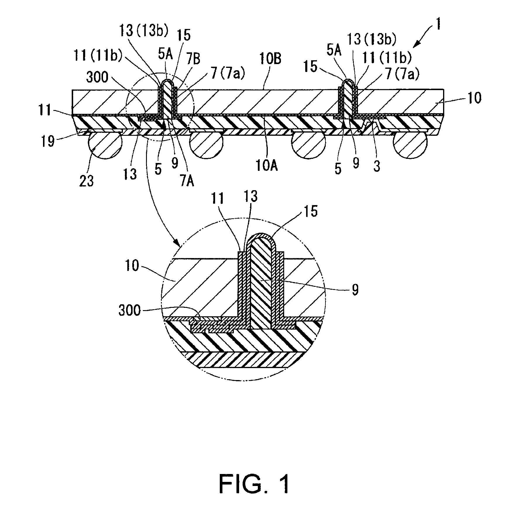
[0055]FIG. 1 is a sectional view showing a schematic configuration of a semiconductor device 1 according to this embodiment.

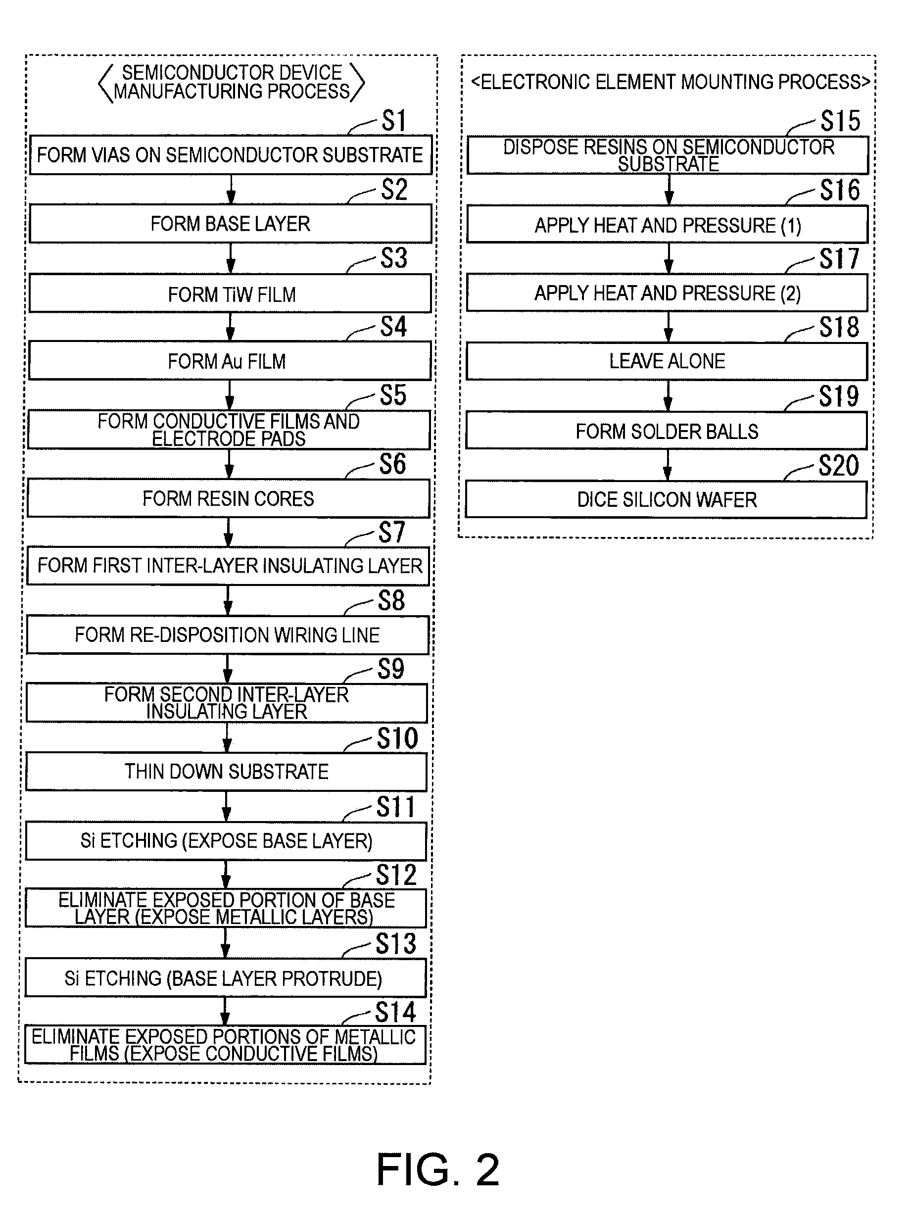
[0056]As shown in FIG. 1, the semiconductor device 1 includes a semiconductor substrate 10 obtained by forming an integrated circuit (not shown) including a transistor, a memory element, and other electronic elements, and the like on one surface of a silicon base material, which is obtained by cutting a silicon wafer, using a known method. Hereafter, a surface having the integrated circuit and the like formed thereon, of the semiconductor substrate 10 will be referred to as an “active surface 10A” and a surface opposite to the active surface 10A will be referred to as a “back surface 10B.” The semiconductor substrate 10 is made of, for example, a rectangular silicon substrate. Instead, for exampl...

second embodiment

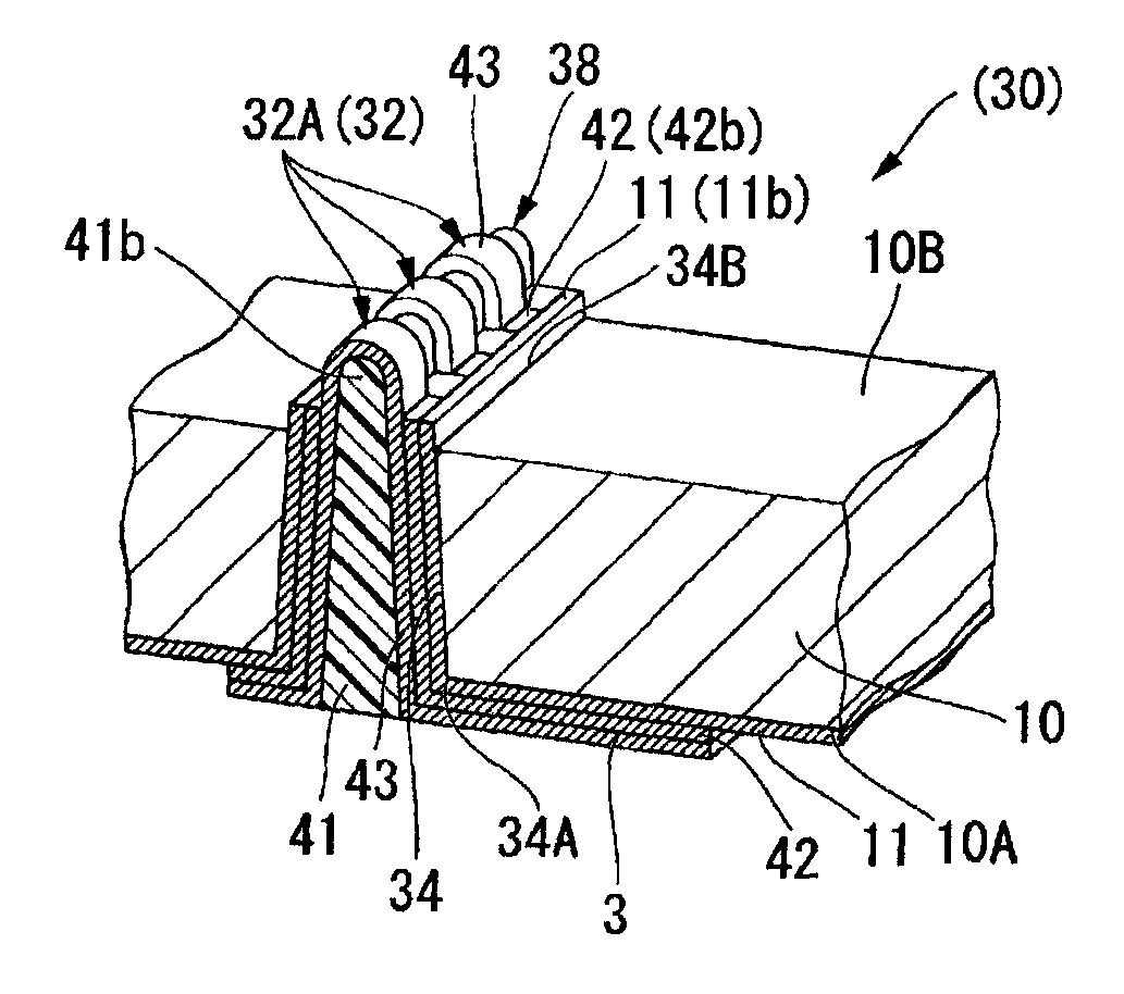
[0106]Next, a second embodiment of the invention will be described. FIG. 8A is a sectional view showing a schematic configuration of a semiconductor device 30 according to the second embodiment. FIG. 8B is an enlarged perspective view showing a connecting portion 38 of the semiconductor device 30 according to the second embodiment. The semiconductor device 30 according to this embodiment to be shown below is approximately the same as the above-mentioned first embodiment except for the configuration of through electrodes 32 (bump electrodes 32A) and the manufacturing method thereof. Accordingly, the through electrodes 32 (bump electrodes 32A) and the manufacturing method thereof will be described in detail and the common elements will not be described. Also, same elements as those in FIGS. 1 to 7 will be assigned same reference numerals in the drawings used for description.

[0107]As shown in FIGS. 8A and 8B, the semiconductor device 30 according to this embodiment includes the connect...


PUM


Abstract

A semiconductor device includes a semiconductor substrate and a through electrode provided in a through hole formed in the semiconductor substrate. The through electrode partially protrudes from a back surface of the semiconductor substrate, which is opposite to an active surface thereof. The through electrode includes a resin core and a conductive film covering at least a part of the resin core.

Description

[0001]This application claims priority to Japanese Patent Application No. 2008-294772 filed on Nov. 18, 2008. The entire disclosure of Japanese Patent Application No. 2008-294772 is hereby incorporated herein by reference.BACKGROUND[0002]1. Technical Field[0003]The present invention relates to a semiconductor device, a manufacturing method thereof, and an electronic apparatus.[0004]2. Related Art[0005]For multilayer semiconductor devices, accurate positioning has been required to bond bumps. For this reason, bonding has been performed by applying heat and pressure using a flip chip bonder. However, there has been a problem that when using solder to bond bumps, the solder overflows from the bonding portions due to the application of heat and pressure and thus a bonding failure easily occurs.[0006]In the configuration described in JP-A-2001-53218, an insulating film is formed on side surfaces of back surface terminals protruding from a silicon substrate. For this reason, at the time o...

Claims


Application Information

Patent Timeline
Patent Type & Authority Patents(United States)
IPC IPC(8): H01L29/40
CPCH01L21/6835H01L24/13H01L23/481H01L24/11H01L24/12H01L24/16H01L21/76898H01L24/90H01L2224/13009H01L2224/13099H01L2224/83191H01L2224/83194H01L2224/83856H01L2224/90H01L2924/01013H01L2924/01015H01L2924/01022H01L2924/01029H01L2924/01046H01L2924/01047H01L2924/01074H01L2924/01075H01L2924/01078H01L2924/01079H01L2924/01082H01L2924/09701H01L2924/14H01L2924/01005H01L2924/01006H01L2924/01019H01L2924/01024H01L2924/01033H01L2924/01072H01L2924/014H01L2224/73103H01L2224/81005H01L2924/00013H01L2924/00012H01L2224/29099H01L2924/15787H01L2924/15788H01L2924/12042H01L2224/73204H01L2224/023H01L2924/00H01L2924/0001
Inventor YODA, TSUYOSHIHARA, KAZUMI
Owner ADVANCED INTERCONNECT SYST LTD
Why Eureka
Try Eureka