Semiconductor test interface

a test interface and semiconductor technology, applied in the direction of electronic circuit testing, measurement devices, instruments, etc., can solve the problems of reducing the service life affecting the reliability of the test interface, so as to facilitate maintenance and high-speed transmission of the test interface. , the effect of reducing the number of connector contact points

Active Publication Date: 2007-10-30
UNITEST
View PDF6 Cites 4 Cited by
  • Summary
  • Abstract
  • Description
  • Claims
  • Application Information

AI Technical Summary

Benefits of technology

[0028]It is an object of the present invention to provide a semiconductor test interface wherein the number of the connector contact points is minimized, the signal integrity of the high-speed transmission signal is improved and the maintenance of the semiconductor test interface is facilitated by simplifying the semiconductor test interface, thereby reducing the manufacturing cost by simplifying the manufacturing process and easily corresponding to the test of the different DUTs.

Problems solved by technology

The configuration disclosed in Korean Patent Application No. 10-1997-0040701 overcomes a disadvantage of conventional semiconductor test interface wherein a configuration of a DUT unit or a base unit thereof is complex, and a maintenance and high-speed transmission of high frequency signal are difficult due to a connection using a soldering or a pogo pin.
However, while the configuration disclosed in Korean Patent Application No. 10-1997-0040701 is advantageous in that the number of contact points such as a solder is less than the conventional configuration, it is disadvantageous to the high-speed signal transmission.
Moreover, while the integrated connector is advantageous to a mechanical contact and support, the integrated connector is disadvantageous in that a high frequency wave characteristic is degraded.
In addition, in accordance with an aspect of the maintenance of the semiconductor test equipment, since the semiconductor test equipment is divided into the base unit and the DUT unit, each of the units should be separately maintained, thereby making a manufacturing process more complex and increasing a manufacturing cost.
However, in accordance with the configuration, a manufacturing cost is increased due to an addition of a board spacer 280 and a maintenance thereof is difficult.

Method used


Image

  • Semiconductor test interface
  • Semiconductor test interface
  • Semiconductor test interface

Examples


Embodiment Construction

[0036]Embodiments in accordance with the present invention will now be described in detail with reference to the accompanied drawings.

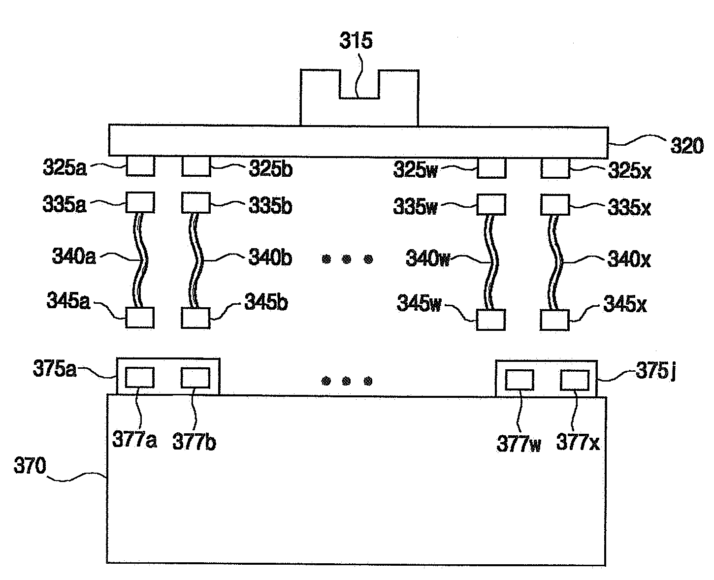
[0037]FIG. 3 is a diagram illustrating a configuration of a semiconductor test interface in accordance with the present invention.

[0038]As shown, the semiconductor test interface in accordance with the present invention may be divided into a DUT unit 310 and a base unit 330, and comprises a DUT board 320 including a test socket 315 for mounting a DUT and a first connector 325a and a cable 340a having a second connector 335a and a third connector 345a at two end portions thereof respectively. It should be noted that the connectors 325a 335a and 345a of the present invention refers to a socket, receptacle or a general connector having a conductive material for an electrical connection therein.

[0039]While the DUT board 320 may comprise one or more test sockets 315 and one or more first connectors, description will be focused on a case of the single test ...


PUM


Abstract

The present invention relates to a semiconductor test interface for interfacing a DUT (Device Under Test) to a pin card using a cable comprising a DUT board including one or more first connectors for electrically connecting one or more test sockets for mounting the DUT to the one or more cables, and a circuit wiring for electrically connecting the one or more test sockets to the one or more first connectors; and the one more cable including a second connector for an electrical connection to the one or more first connectors, and a third connector for an electrical connection to the pin card, wherein the one or more first connectors correspond to the one or more cables by 1:1.In accordance with the present invention, the manufacturing cost is reduced by simplifying the manufacturing process and the semiconductor test interface may easily correspond to the test of the different DUTs.

Description

RELATED APPLICATIONS [0001]The present disclosure relates to subject matter contained in priority Korean Application No. 10-2005-0049869 filed on 10 Jun. 2005, which is herein expressly incorporated by reference in its entirety.BACKGROUND OF THE INVENTION[0002]1. Field of the Invention[0003]The present invention relates to a semiconductor test interface, and more particularly, to a semiconductor test interface for performing a test of a semiconductor device by connecting the semiconductor device to be tested to the semiconductor test equipment.[0004]2. Description of the Related Art[0005]Generally, a test of a semiconductor chip is a final process for determining whether a complete product is a defective product. Semiconductor test equipments for effectively testing multiple products have been developed and are being used.[0006]FIG. 1a is a diagram illustrating an example of a conventional semiconductor test equipment.[0007]As shown, the conventional semiconductor test interface com...

Claims


Application Information

Patent Timeline
Patent Type & Authority Patents(United States)
IPC IPC(8): G01R31/02G01R31/28
CPCG01R31/2889G01R31/28
Inventor KIM, DAE KYOUNGKIM, SUN WHANLEE, DAL JO
Owner UNITEST
Why Eureka
Try Eureka