Method for making multilayer connection structure

a multi-layer connection and structure technology, applied in the direction of semiconductor devices, semiconductor/solid-state device details, electrical equipment, etc., can solve the problems of increasing the cost of interconnection implementation with the number of lithographic steps, and using a separate mask

Active Publication Date: 2013-02-26
MACRONIX INT CO LTD
View PDF21 Cites 74 Cited by
  • Summary
  • Abstract
  • Description
  • Claims
  • Application Information

AI Technical Summary

Problems solved by technology

The cost to implement the interconnections increases with the number of lithographic steps needed.
However, one of the drawbacks with conventional 3-D stacked memory devices is that a separate mask is typically used for each contact level.

Method used


Image

  • Method for making multilayer connection structure
  • Method for making multilayer connection structure
  • Method for making multilayer connection structure

Examples


Embodiment Construction

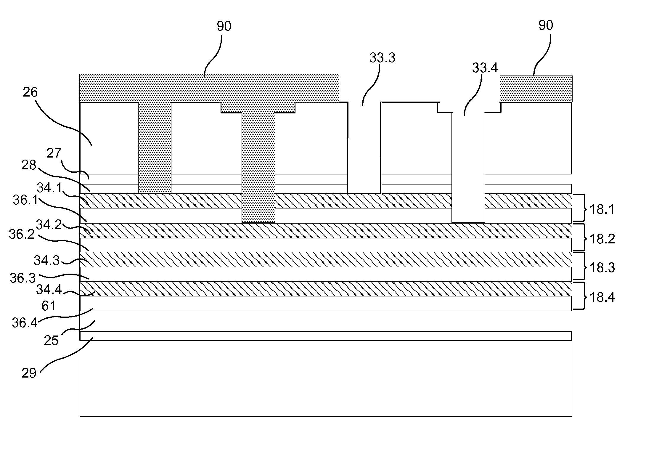
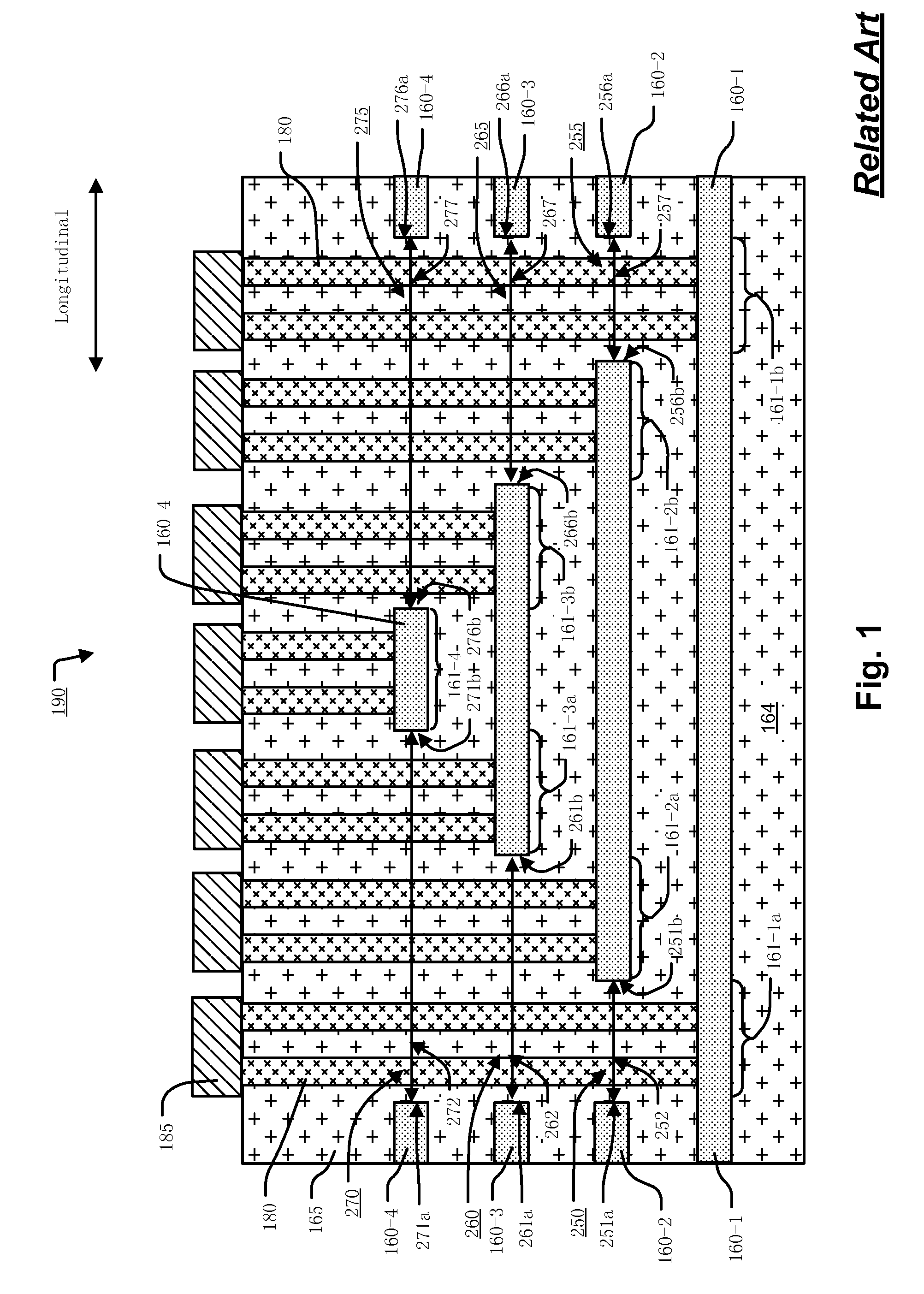
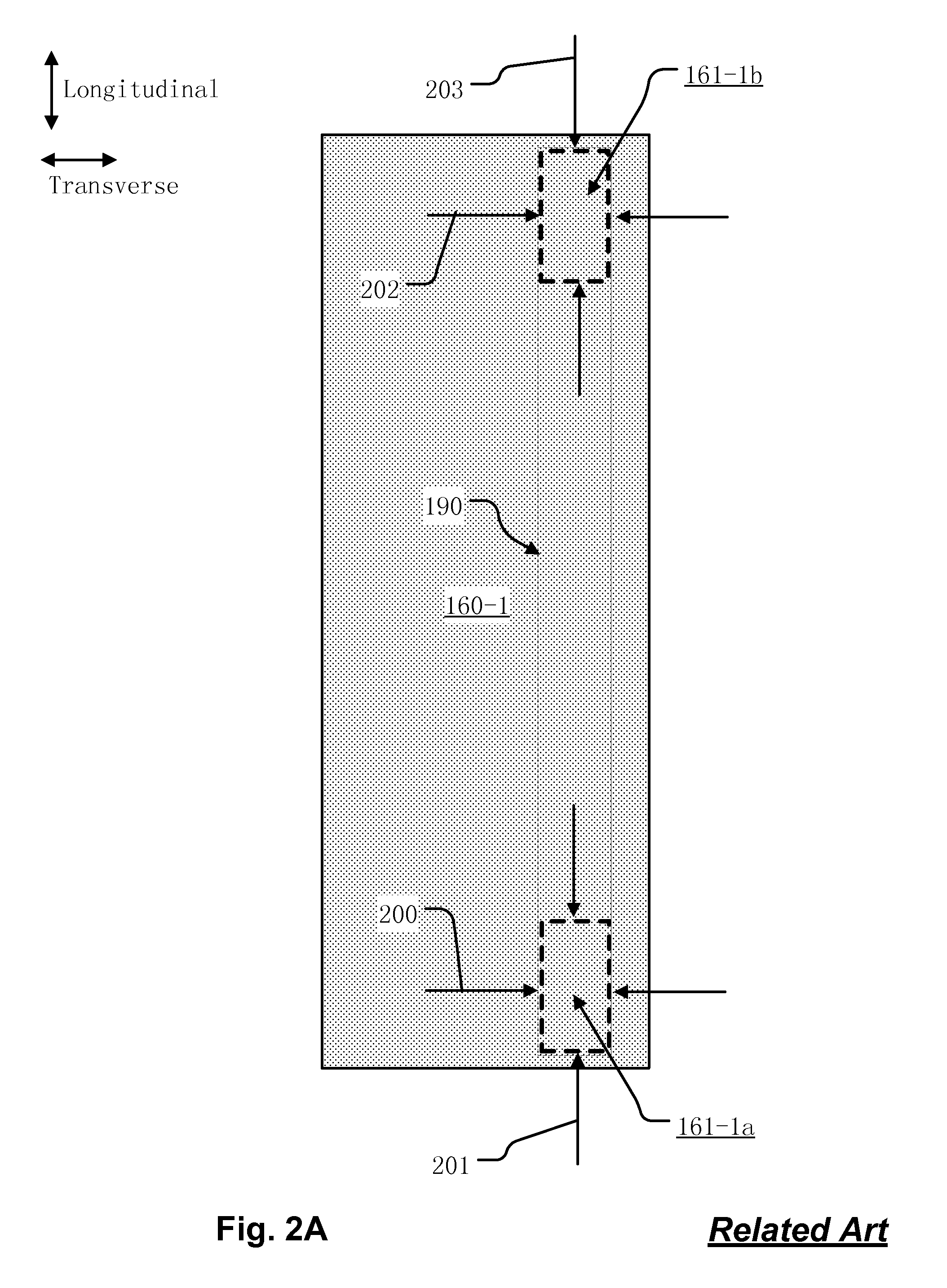
[0053]FIG. 1 illustrates a cross-sectional view of a device including three-dimensional structure having an interconnect structure 190 with a small footprint where conductors 180 extend to various levels 160-1 to 160-4 in the device. In the illustrated example, four levels 160-1 to 160-4 are shown. More generally, the small interconnect structure 190 described herein can be implemented in a structure having levels 0 to N, where N is at least 2.

[0054]The conductors 180 are arranged within the interconnect structure 190 to contact landing areas on the various levels 160-1 to 160-4. As described in more detail below, the conductors 180 for each particular level extend through openings in the overlying levels to contact the landing areas 161-1a, 161-1b, 161-2a, 161-2b, 161-3a, 161-3b, 161-4. The conductors 180 are used, in this example, for coupling the contact levels 160-1 to 160-4 to interconnect lines 185 in a wiring layer overlying the levels 160-1 to 160-4.

[0055]The landing areas a...


PUM


Abstract

A method provides electrical connections to a stack of contact levels of an interconnect region for a 3-D stacked IC device. Each contact level comprises conductive and insulation layers. A portion of any upper layer is removed to expose a first contact level and create contact openings for each contact level. A set of N masks is used to etch the contact openings up to and including 2N contact levels. Each mask is used to etch effectively half of the contact openings. When N is 3, a first mask etches one contact level, a second mask etches two contact levels, and a third mask etches four contact levels. A dielectric layer may be formed on the sidewalls of the contact openings. Electrical conductors may be formed through the contact openings with the dielectric layers electrically insulating the electrical conductors from the sidewalls.

Description

CROSS-REFERENCE TO RELATED APPLICATIONS[0001]This application claims the benefit of U.S. provisional patent application No. 61 / 434,423 filed 19 Jan. 2011.[0002]This application is related to U.S. provisional patent application No. 61 / 434,086 filed 19 Jan. 2011; and U.S. patent application Ser. No. 12 / 579,192 filed 14 Oct. 2009.BACKGROUND OF THE INVENTION[0003]1. Field of the Invention[0004]The present invention relates generally to high density integrated circuit devices, and more particularly to interconnect structures for multi-level three-dimensional stacked devices.[0005]2. Description of Related Art[0006]In the manufacturing of high density memory devices, the amount of data per unit area on an integrated circuit can be a critical factor. Thus, as the critical dimensions of the memory devices approach lithographic technology limits, techniques for stacking multiple levels of memory cells have been proposed in order to achieve greater storage density and lower costs per bit.[000...

Claims


Application Information

Patent Timeline
Patent Type & Authority Patents(United States)
IPC IPC(8): H01L21/4763H01L21/44
CPCH01L23/50H01L27/11286H01L23/5226H01L21/76805H01L27/0207H01L21/76816H01L21/76831H01L21/76838H01L27/11206H01L27/11565H01L27/11578H01L27/11582H01L24/19H01L2924/1306H01L27/0688H01L2924/00H01L2924/14H10B20/60H10B20/20H10B43/10H10B43/20H10B43/27H01L23/522H01L23/481
Inventor CHEN, SHIH-HUNGLUE, HANG-TINGLEE, HONG-JIYANG, CHIN-CHENG
Owner MACRONIX INT CO LTD
Why Eureka
Try Eureka