Solid-state imaging device, method of manufacturing the same, and camera

a solid-state imaging and manufacturing method technology, applied in the field of solid-state imaging devices, can solve the problems of reducing sensitivity, increasing color-mixing, and insufficient light collected by the on-chip microlens, and achieves the effects of suppressing color-mixing, improving sensitivity, and high image quality

Inactive Publication Date: 2013-03-12
SONY CORP
View PDF19 Cites 19 Cited by
  • Summary
  • Abstract
  • Description
  • Claims
  • Application Information

AI Technical Summary

Benefits of technology

[0026]As shown in FIG. 1, the above-described CMOS image sensor 11 including the optical inner filter layer 12 in the layer under the color filter 7 has a larger distance H1 from the light-receiving surface of the photodiode (PD) 3 to the on-chip microlens 8, compared with the distance H2 of the CMOS image sensor 1 without the optical inner filter layer 12 as shown in FIG. 2. An increase in distance H1 leads to a decrease in probability of incident light to reach the photodiode (PD) 3. In addition, insufficient light may be collected by the on-chip microlens 8. Thus, color light incident on a target pixel by passing through the color filter, particularly oblique light L′ tends to enter any adjacent pixel for another color. Therefore, there is a possibility of lowering the sensitivity and increasing color-mixing.
[0027]It is desirable to provide a solid-state imaging device including an optical inner filter layer blocking infrared light, having improved sensitivity and suppressing the occurrence of color-mixing. It is also desirable to provide a camera module including such a solid-state imaging device.

Problems solved by technology

In addition, insufficient light may be collected by the on-chip microlens 8.
Therefore, there is a possibility of lowering the sensitivity and increasing color-mixing.
However, there are two disadvantages for industrial production; the disadvantages are of color-mixing and ripples (little undulations or waves).

Method used


Image

  • Solid-state imaging device, method of manufacturing the same, and camera
  • Solid-state imaging device, method of manufacturing the same, and camera
  • Solid-state imaging device, method of manufacturing the same, and camera

Examples


first embodiment

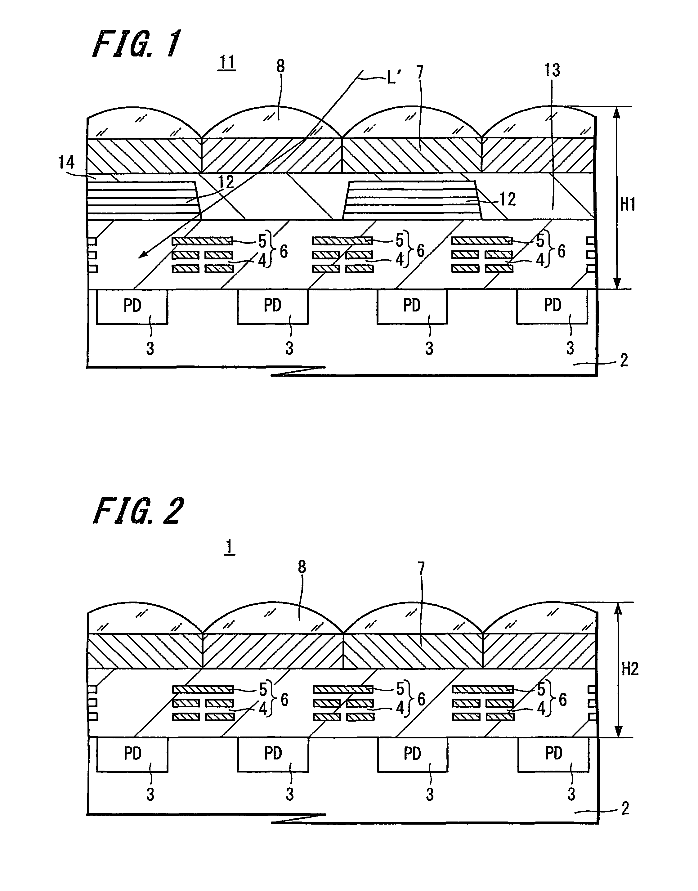
[0122]Next, FIG. 7 illustrates a cross-sectional structure of main parts of a CMOS solid-state imaging device according to the present invention. In order to describe an embodiment of the present invention to be understandable, a pixel is represented only by a photodiode (PD) 31 and schematically described while omitting pixel transistors. The same will be applied to each of other embodiments described later.

[0123]As shown in FIG. 7, a CMOS solid-state imaging device 71 according to the first embodiment includes a plurality of pixels 22, each having the photodiode (PD) 31, arranged in a two-dimensional array on the principal surface of a semiconductor substrate 100. In addition, a plurality of wiring layers 55 are formed on the semiconductor substrate 100 through an insulating interlayer 53. In this example, three layered lines 54 [541, 542, and 543] form the plurality of wiring layers 55. An inner-layer lens 72 is formed corresponding to the respective pixels 22 above the plurality...

second embodiment

[0138]FIG. 11 illustrates a CMOS solid-state imaging device according to the present invention.

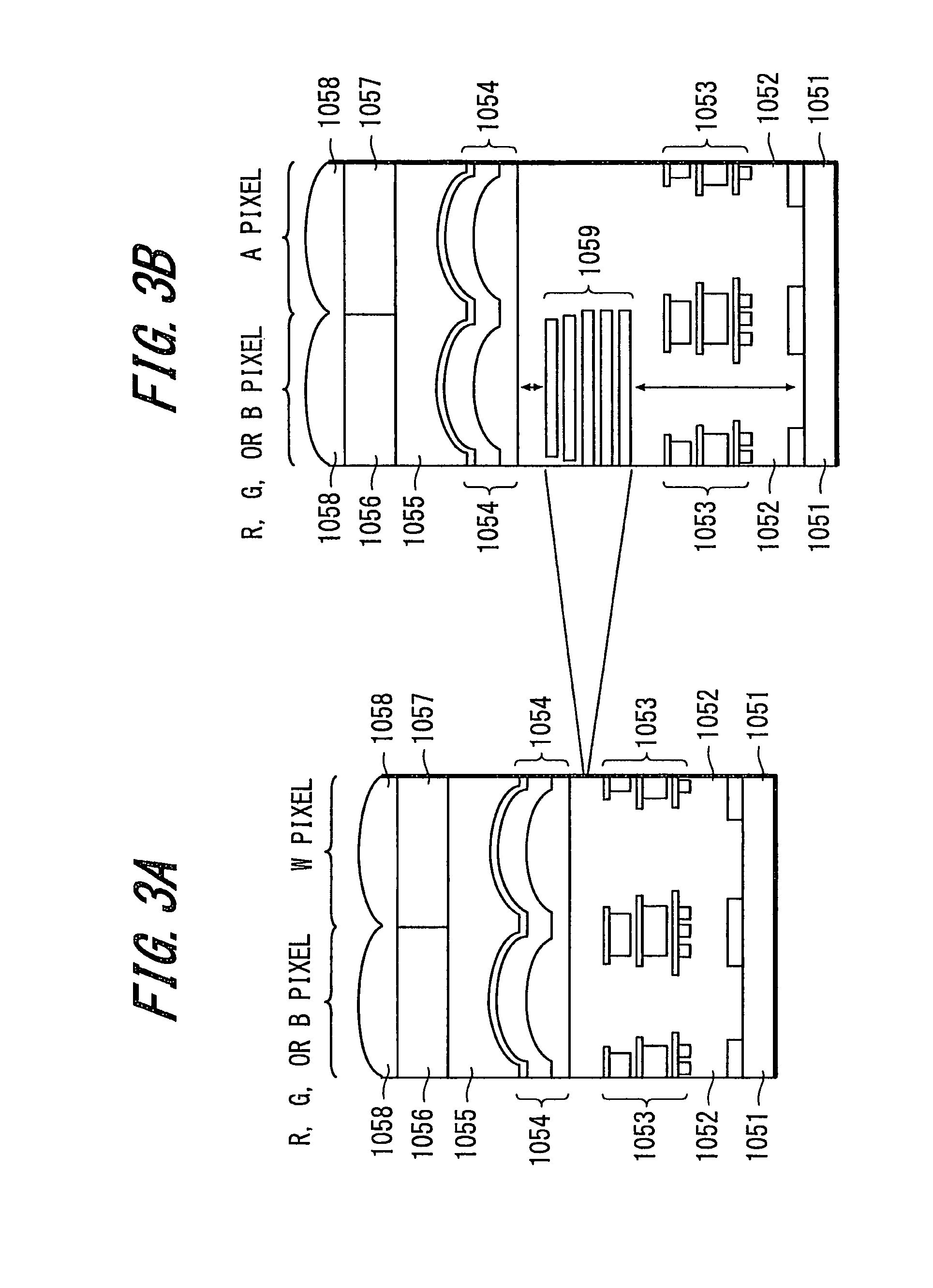
[0139]In a CMOS solid-state imaging device 77 of the present embodiment, a buried layer for filling between optical inner filer layers 62 and a planarizing layer are integrally formed with an organic film 81. Here, other structural components are similar to those in FIG. 7 as described above. Therefore, the same structural components in FIG. 11 are designated by the same reference numerals of the corresponding components in FIG. 7 and their duplicate descriptions will be omitted.

[0140]In the CMOS solid-state imaging device 77 of the second embodiment, the organic film 81 filling space between the adjacent optical inner filter layers 62 can also function as a planarizing layer on the layers 62. Thus, it leads to a reduction in number of manufacturing steps and a reduction in distance between the light-receiving surface and the on-chip microlens or a reduction in layer thickness, as well as ...

third embodiment

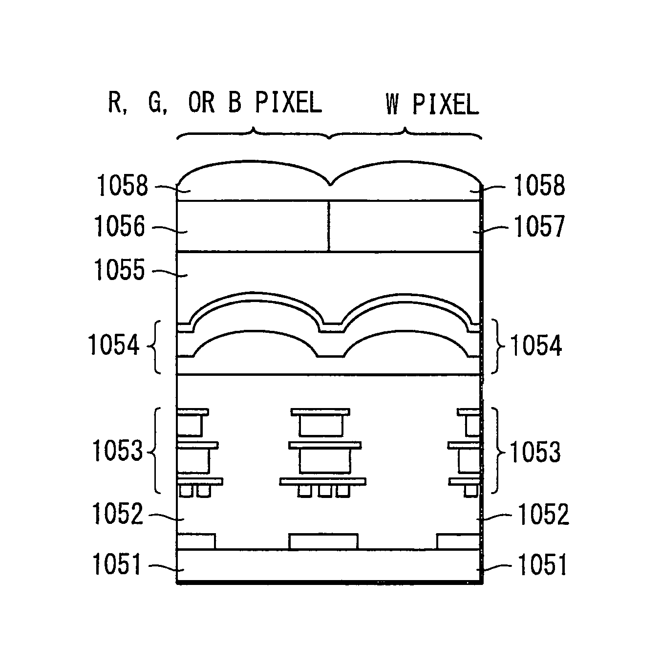
[0141]FIG. 12 illustrates a CMOS solid-state imaging device according to the present invention. In a CMOS solid-state imaging device 78 of the present embodiment, optical inner filter layers 62 have a lens shape copied from the lens shape of the corresponding inner-layer lens 72. In other words, an insulating interlayer 53, an upwardly-convex first interlayer film 73, and a second interlayer film 74 extending along the upper surface of the first interlayer film 73 form the inner-layer lens 72. In addition, the lens-shaped optical inner filter layer 62 is formed on the second interlayer film 74. Other structural components are the same as those represented in FIG. 7 as described above. Thus, these structural components in FIG. 12 are designated by the same reference numerals of the corresponding components in FIG. 7 and their duplicate descriptions will be omitted.

[0142]As described above, in the CMOS solid-state imaging device 78 according to the third embodiment, each of the optica...


PUM


Abstract

A solid-state imaging device is provided. The solid-state imaging device includes a plurality of arrayed pixels, an optical inner filter layer, and an inner-layer lens. Each of the plurality of arrayed pixels includes a photoelectric conversion portion and a pixel transistor. The optical inner filter layer is configured to block infrared light and faces a light-receiving surface of the photoelectric conversion portion of a desired pixel among the arrayed pixels. The inner-layer lens is formed below the optical inner filter layer.

Description

CROSS REFERENCES TO RELATED APPLICATIONS[0001]The present invention contains subject matter related to Japanese Patent Application JP 2007-316280 filed on Dec. 6, 2007 and Japanese Patent Application JP 2008-113016 filed on Apr. 23, 2008, in the Japanese Patent Office respectively, the entire contents of which being incorporated herein by reference.BACKGROUND OF THE INVENTION[0002]1. Field of the Invention[0003]The present invention relates to a solid-state imaging device, for example a MOS image sensor, a method of manufacturing the same, and a camera using such a solid-state imaging device.[0004]2. Description of the Related Art[0005]Solid-state imaging devices can be roughly classified into charge transfer solid-state imaging devices typified by CCD image sensors and amplified solid-state imaging devices typified by CMOS image sensors. In comparison with the CMOS image sensor, the CCD image sensor may need a power supply voltage higher than that of the CMOS image sensor, because ...

Claims


Application Information

Patent Timeline
Patent Type & Authority Patents(United States)
IPC IPC(8): H04N3/14H04N5/335
CPCH01L27/14621H01L27/14627H04N9/045H01L27/14685H01L27/14645H04N25/131H04N25/135
Inventor TATANI, KEIJIRENNIE, JOHNINOUE, SUSUMUTODA, ATSUSHI
Owner SONY CORP
Why Eureka
Try Eureka