Band-pass structure electrostatic discharge protection circuit

a protection circuit and bandpass technology, applied in emergency protection arrangements for limiting excess voltage/current, electrical devices, and arrangements responsive to excess voltage, etc., can solve the problems of rf circuit performance degradation, rf transceiver circuit or sub-circuit damage by electrostatic discharge, etc., to improve the esd robustness of the rf core circuit, reduce chip area, and high performan

Active Publication Date: 2013-07-09
NAT TAIWAN UNIV
View PDF11 Cites 6 Cited by
  • Summary
  • Abstract
  • Description
  • Claims
  • Application Information

AI Technical Summary

Benefits of technology

[0012]It is another objective of the present invention to provide a band-pass structure ESD protection circuit comprising a plurality of diodes and two inductors, wherein the plurality of diodes construct a plurality of positive ESD paths and a plurality of negative ESD paths. The diodes and inductors are configured to form a band-pass filter for improving the ESD robustness of the RF core circuit.
[0013]It is another objective of the present invention to provide a band-pass structure ESD protection circuit ensuring the RF core circuit high performance under high ESD stress.
[0014]It is another objective of the present invention to provide a band-pass structure ESD protection circuit using spiral inductors for reducing chip area and improving the ESD robustness of the RF core circuit.

Problems solved by technology

Thus, it is possible for the RF transceiver circuit or sub-circuit to be damaged by the electrostatic discharge (ESD) that occurs in the environment because of the weather or other artificial interference.
On the other hand, if there are more diodes used as ESD paths in the ESD protection circuit, the larger the parasitic capacitance is, and the performance of the RF circuit will be degraded much seriously.

Method used


Image

  • Band-pass structure electrostatic discharge protection circuit
  • Band-pass structure electrostatic discharge protection circuit
  • Band-pass structure electrostatic discharge protection circuit

Examples


Embodiment Construction

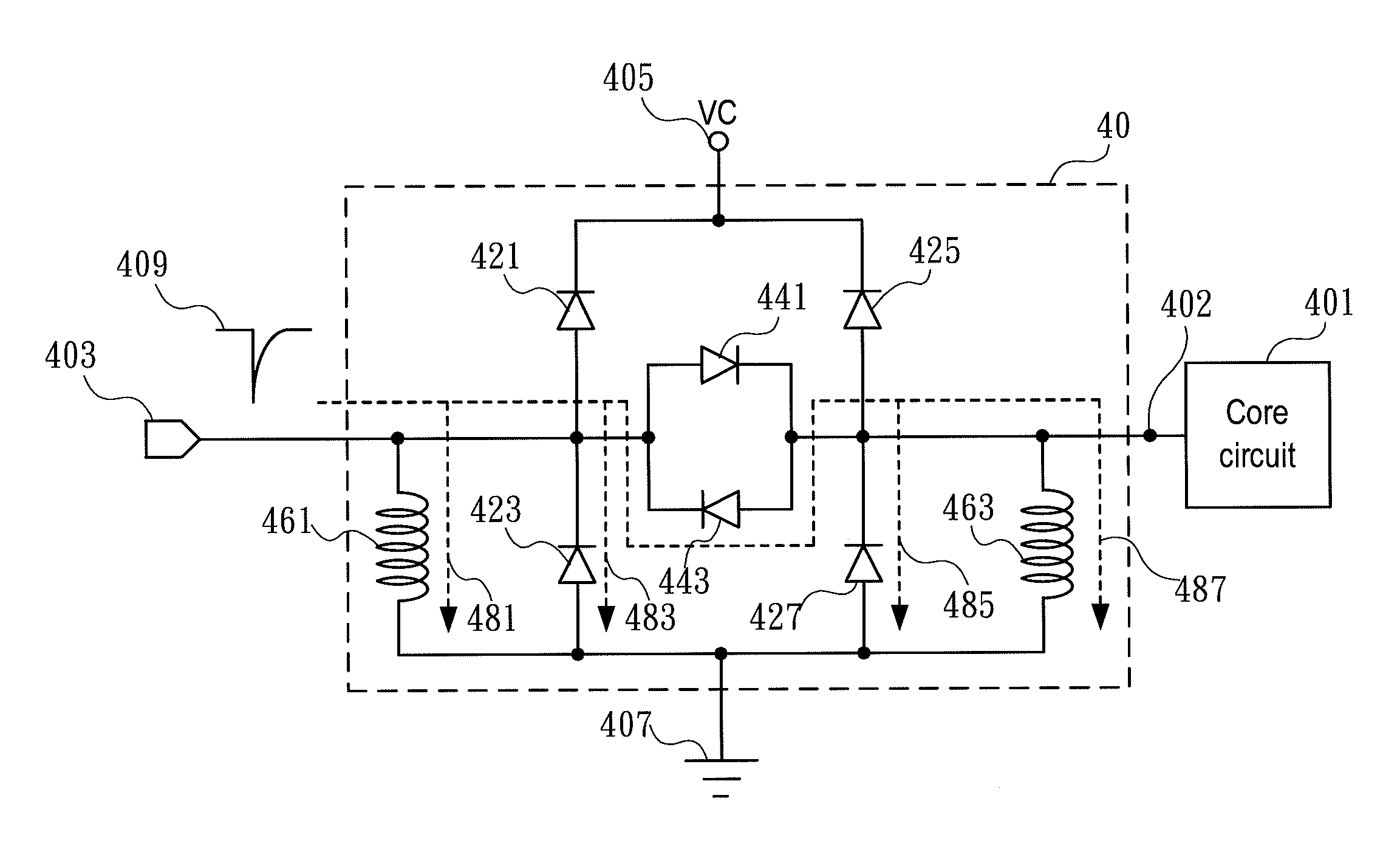
[0033]Referring to FIG. 4, there is shown a schematic diagram of an ESD protection circuit in accordance with one embodiment of the present invention. The band-pass structure ESD protection circuit 40 comprises a first diode 421, a second diode 423, a third diode 425, a fourth diode 427, a fifth diode 441, a sixth diode 443, a first inductor 461, and a second inductor 463.

[0034]The first diode 421 is connected between a power source 405 and an external pad 403, the second diode 423 is connected between the external pad 403 and the ground 407. The third diode 425 is connected between the power source 405 and the I / O port 402 of the RF core circuit 401, the fourth diode 427 is connected between the I / O port 402 and the ground 407. The first diode 421 and the second diode 423 are connected in series. The third diode 425 and the fourth diode 427 are connected in series.

[0035]The fifth diode 441 and the sixth diode 443 are connected between the external pad 403 and the I / O port 402 rever...


PUM


Abstract

The present invention relates to an electrostatic discharge (ESD) protection circuit, and more particularly to a band-pass structure electrostatic discharge protection circuit. An ESD protection circuit is disposed at the input of a radio frequency (RF) core circuit. The ESD protection circuit comprises a plurality of diodes and inductors constructing a plurality of discharging paths, wherein the diodes and inductors forms a band-pass filter structure. Such that, the RF core circuit with the ESD protection circuit of the present invention feature much higher ESD robustness and better RF performance than the conventional design.

Description

FIELD OF THE INVENTION[0001]The present invention relates to an electrostatic discharge (ESD) protection circuit, and more particularly to a band-pass structure electrostatic discharge protection circuit.BACKGROUND OF THE INVENTION[0002]Nowadays, the wireless communication industry plays a much important role in the economic advancement. A variety of Radio Frequency (RF) circuit designs and researches are provided for improving the efficiency or performance of the RF devices.[0003]With respect to the radio frequency transceiver circuit or sub-circuit, such as a low noise amplifier or a power amplifier, the input / output (I / O) pad is exposed directly to the environment through an antenna or other I / O element. Thus, it is possible for the RF transceiver circuit or sub-circuit to be damaged by the electrostatic discharge (ESD) that occurs in the environment because of the weather or other artificial interference.[0004]A traditional ESD protection circuit is shown in FIG. 1. The ESD prot...

Claims


Application Information

Patent Timeline
Patent Type & Authority Patents(United States)
IPC IPC(8): H02H9/00H02H3/22
CPCH02H9/046
Inventor HUANG, BO-JRWANG, HUEI
Owner NAT TAIWAN UNIV
Why Eureka
Try Eureka