

Transistor with increased ESD robustness and related layout method thereof
a transistor and robustness technology, applied in the field of transistor layout method, can solve the problems of nscr transistor b>50/b> damage, the above layout method is not suited for small area transistor manufacturing, and the effect of increasing esd robustness
- Summary
- Abstract
- Description
- Claims
- Application Information
AI Technical Summary
Benefits of technology
Problems solved by technology
Method used
Image

Examples
Embodiment Construction
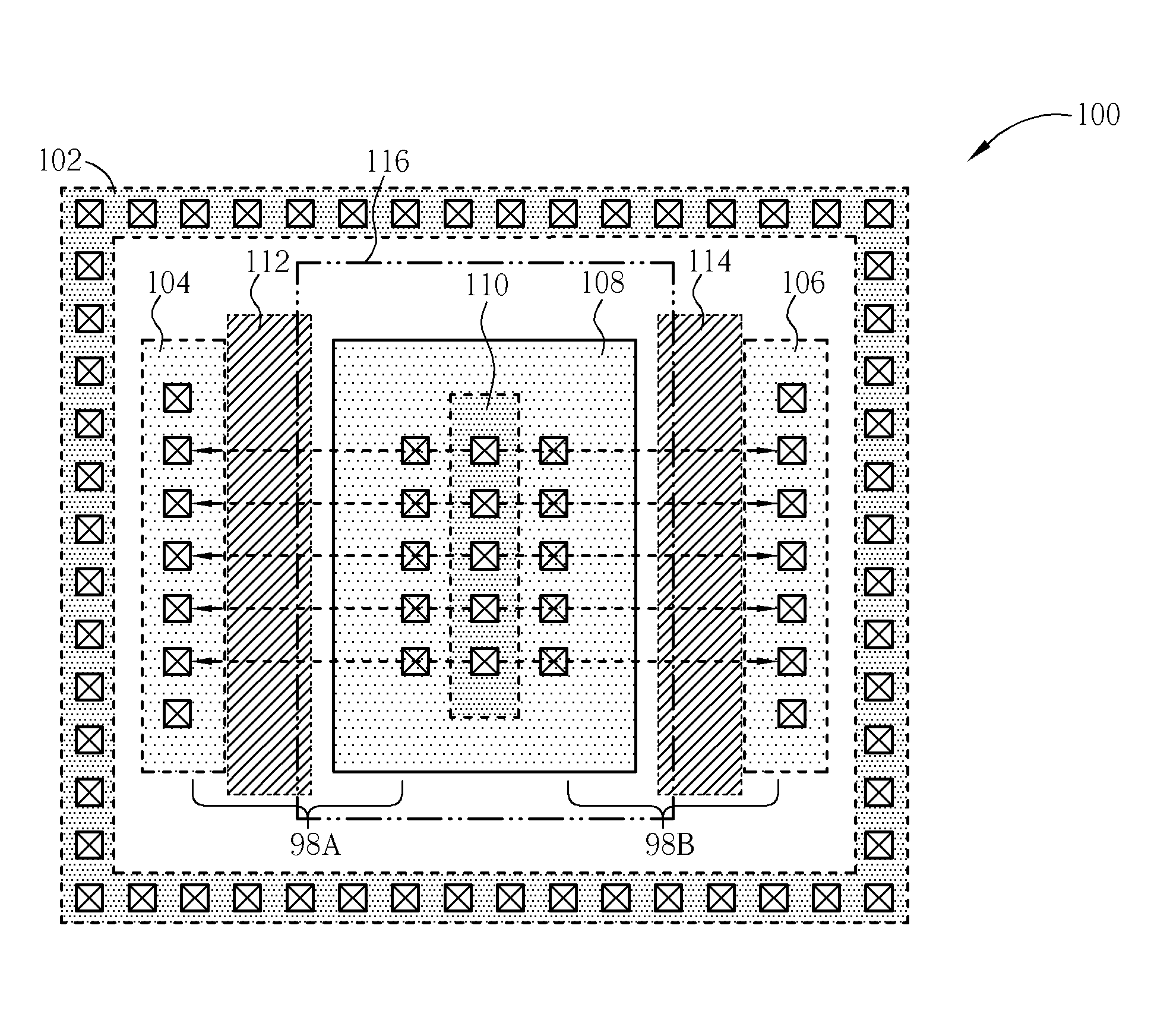
[0017] Please refer to FIG. 4. FIG. 4 is a schematic layout diagram of an NSCR transistor 100 according to an embodiment of the present invention. In this embodiment, the NSCR transistor 100 is a silicon-controlled rectifier cell (SCR cell), which includes NMOS transistors 98A, 98B made from regions 108, 112, 114, 104, and 106, a P type semiconductor substrate (not shown), a P type ring region 102, two rectangular N type diffusion regions 104, 106, an N type ring diffusion region 108, a P type diffusion region 110, and poly-silicon regions 112, 114. The area enclosed by the dotted line 116 includes an N type well being surrounded under an N type ring diffusion 108, P type diffusion region 110, and portions of poly-silicon regions 112, 114. As shown through FIG. 4, the pads of the rectangular N type diffusion region 104, 106, and the P type ring region 102, are coupled to the source of the NSCR transistor 100. The pads of the ring N type diffusion region 108 and the P type diffusion ...
PUM
 Abstract
Description
Claims
Application Information