ESD protection design with turn-on restraining method and structures

a protection circuit and turn-on technology, applied in the direction of semiconductor devices, electrical equipment, semiconductor/solid-state device details, etc., can solve the problems of high cost, increased cost, and serious degradation of cmos integrated circuits (ics), and achieve the reduction of the turn-on speed of the first mos transistor, improve the esd robustness of i/o cells, and increase the drain breakdown voltage

Inactive Publication Date: 2012-02-28
TRANSPACIFIC IP LTD
View PDF52 Cites 5 Cited by
  • Summary
  • Abstract
  • Description
  • Claims
  • Application Information

AI Technical Summary

Benefits of technology

[0022]It is an object of the present invention to provide a semiconductor structure for ESD protection of an integrated circuit in order to improve ESD level of the I / O cells with different driving specifications.
[0023]Another object of the present invention is to provide a semiconductor structure for improving ESD robustness of the output ESD protection NMOS / PMOS through an additional pick-up diffusion region and / or modification of channel length.
[0025]A still further object of the present invention is to provide a semiconductor structure to improve ESD robustness of the I / O cells by using different channel lengths in the I / O devices.
[0026]In accordance with the present invention, a semiconductor structure for electrostatic discharge (ESD) protection of a metal-oxide semiconductor (MOS) integrated circuit consists of a p-type substrate forming a base for the semiconductor structure, a first n-type channel formed between first N+ regions within the substrate for an Mn1 transistor, and a second n-type channel formed between second N+ regions within the substrate for an Mn2 transistor. In particular, an additional P+ pick-up diffusion region is disposed adjacent to the first N+ regions to reduce the turn-on speed of the first MOS transistor. Alternatively or in addition to the P+ pick-up diffusion region, the channel lengths of the first and second n-typ channels can be varied such that the channel length of the first n-type channel is larger than the channel length of the second n-type channel to increase the drain breakdown voltage of the first MOS transistor.

Problems solved by technology

The ESD robustness of CMOS integrated circuits (IC) has been found to be seriously degraded due to deep-submicron CMOS technologies.
This creates a challenge to provide one set of I / O cells with better ESD level.
Although such design methodology can improve the ESD level of the I / O library, it is costly and requires additional elements to realize the gate-coupled circuit or modifications to lower the junction breakdown voltage.

Method used


Image

  • ESD protection design with turn-on restraining method and structures
  • ESD protection design with turn-on restraining method and structures
  • ESD protection design with turn-on restraining method and structures

Examples


Embodiment Construction

[0054]The present invention will now be described by way of preferred embodiments with references to the accompanying drawings. Like numerals refer to corresponding parts of various drawings.

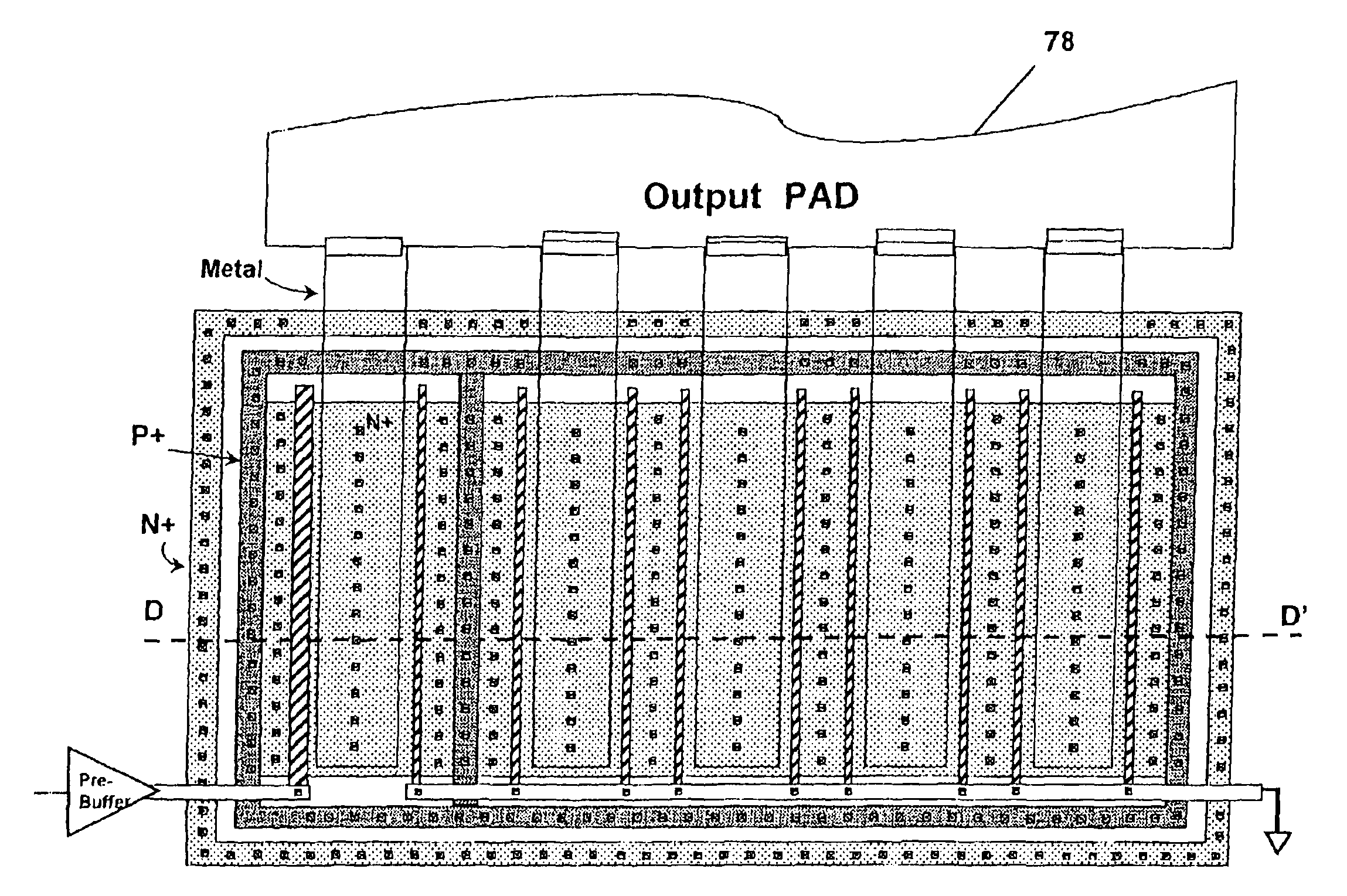
[0055]Referring now to FIGS. 7(a) and 7(b), one embodiment of the present invention is shown in which a simple layout is employed for drawing an additional P+ pick-up diffusion region 70, which surrounds one of the MOS transistors (Mn1 guarded device) 72 to reduce its parasitic base-emitter resistance. Therefore, the parasitic BJT in Mn1 has a slower turn-on speed than that of the other MOS transistor (Mn2 ESD protection device) 74. As shown in FIG. 7(b), a pre-buffer 76 with a core logic 77 is connected to the Mn1 device 72, a pad 78 is connected to the Mn1 device 72 and Mn2 device 74, and an ESD current discharging path is indicated by dash lines when the turn-on speed of Mn1 device 72 is slowed down. A corresponding top layout view is shown in FIG. 7(c) in which a cross-sectional view along t...


PUM


Abstract

The present invention is directed to an electrostatic discharge (ESD) device with an improved ESD robustness for protecting output buffers in I / O cell libraries. The ESD device according to the present invention uses a novel I / O cell layout structure for implementing a turn-on restrained method that reduces the turn-on speed of an ESD guarded MOS transistor by adding a pick-up diffusion region and / or varying channel lengths in the layout structure.

Description

BACKGROUND OF THE INVENTION[0001]1. Field of the Invention[0002]The present invention is directed generally to electrostatic discharge (ESD) protection circuits for input / output (I / O) devices, and more particularly, to improving ESD robustness in I / O cell libraries using novel layout techniques to implement a turn-on retraining arrangement that reduces the turn-on speed or increases the breakdown voltage of a MOS transistor.[0003]2. Description of the Related Art[0004]The ESD robustness of CMOS integrated circuits (IC) has been found to be seriously degraded due to deep-submicron CMOS technologies. To improve the ESD robustness of the output transistors, the ESD-implant process and the silicide-blocking process have been widely implemented in the deep-submicron CMOS technologies. In addition to the process modification to improve the ESD robustness of the output buffers, the symmetrical layout structure had been emphasized to realize the large-dimension output transistors by ensurin...

Claims


Application Information

Patent Timeline
Patent Type & Authority Patents(United States)
IPC IPC(8): H01L23/62H01L27/02
CPCH01L27/0277H01L2924/0002H01L2924/00
Inventor KER, MING-DOUPENG, JENG-JIEJIANG, HSIN-CHIN
Owner TRANSPACIFIC IP LTD
Why Eureka
Try Eureka