However, uniformity of
electric field cannot be maintained perfectly and the uniformity of the
glow discharge and henceforth wear on the target is influenced by a number of factors, including thermal currents generated in the chamber and other mechanical anomalies, such as target misalignment.
Even with the rotating
magnet mechanism in place to attempt to stabilize the
glow discharge, certain conditions can result in a local concentration of the
electric field causing the
glow discharge to pass from the superconducting region of the Paschen curve into the arcing region.
Arcing during PVD results in an unintended
low impedance path from the
anode to the target through electrons or ions in the
plasma, the unintended path generally including ground, with the arcing being caused by factors such as
contamination (i.e., inclusions) of the target material, inclusions within the structure (e.g., surface) of the target, improper target alignment (e.g., misalignment of
cathode and
anode), vacuum leaks, and / or
contamination from other sources such as
vacuum grease.
Arcing during PVD is one cause of yield-reducing defects in forming integrated circuits on
semiconductor wafers.
The dislodged
solid piece of target material may be large relative to the thickness of the uniform
coating expected on the
wafer, and if a large piece falls upon the
wafer, it may cause a defect in the
integrated circuit being formed at that location.
Because arcing results in a localized defect (area) having a greater thickness than the surrounding
metal, the defect area may not be thoroughly etched in the subsequent
processing, resulting in an unintended circuit path (i.e., short) on the
chip.
A local defect in one layer can also distort an overlying pattern imaged onto the
wafer in a subsequent
photolithography step, and thus result in a defect in an overlying layer.
Arcing in a PVD
sputtering apparatus used to process wafers into integrated circuits can render portions of the wafer useless for its intended purpose, thereby increasing manufacturing costs.
Using target materials free of arc-causing inclusions is one way of minimizing
integrated circuit fabrication defects; however, target material may become contaminated during its manufacture or thereafter.
Discovering target
contamination prior to
sputtering operations so as to prevent arcing defects is costly, both in terms of time and expense.
Not discovering arcing defects in a timely manner is similarly costly in terms of random yield loss, for example by the manufacturer operating a
deposition chamber until the target inclusion causing the arcing is sputtered through.
Furthermore, when a
solid piece of the target is dislodged during an arc, the surface of the target may be further damaged and the potential for future arcing in that neighborhood increases.
It is costly to measure the number of defective
layers caused by arcing, for example via electrical tests designed to reveal shorts or by scanning the surface of wafers with a
laser after
metal deposition.
These tests take time to run, during which production is delayed, or undetected yield loss occurs for an
extended time.
When this occurs, the presence of series
inductance in the driving point impedance of the power
delivery system, comprising power supply and
interconnection means, causes a rapid drop in the magnitude of observed
voltage between the
anode and cathode of the chamber.
As such, such a system may miss arcs of
small magnitude, which nonetheless cause damage.
Electronically controlled analog or
switching power supplies cannot react to this rapid change in chamber impedance during a microarc.
While useful for gaining an understanding of the arcing phenomenon in PVD applications, this method of computing arcs and
arc energy using an
oscilloscope and a post
processing computer is of little value in production applications.
Even modern handheld oscilloscopes are relatively bulky instruments, and real estate in an integrated circuit clean room is extremely valuable.
A stand alone post
processing computer also takes up valuable floor space and would likely need to be located outside the clean room and connected to the
oscilloscope by a network, adding latency in the transfer of data between the
oscilloscope and computer.
Furthermore, there is no means to tell a-priori the duration of an individual arc, or the frequency at which they might occur, leaving the problem of exactly how to set the controls of the oscilloscope.
Oscilloscopes also have limited waveform storage capability, and therefore prone to losing information at the times in which it is needed most, when there is much arcing activity during a process.
In addition to the problems discussed, when counting arcs only as
voltage threshold violations, some information may be lost or obscured if the power supply responds to the arcs by reducing delivered power.
The result of reducing power is a dip in both the
voltage and the current.
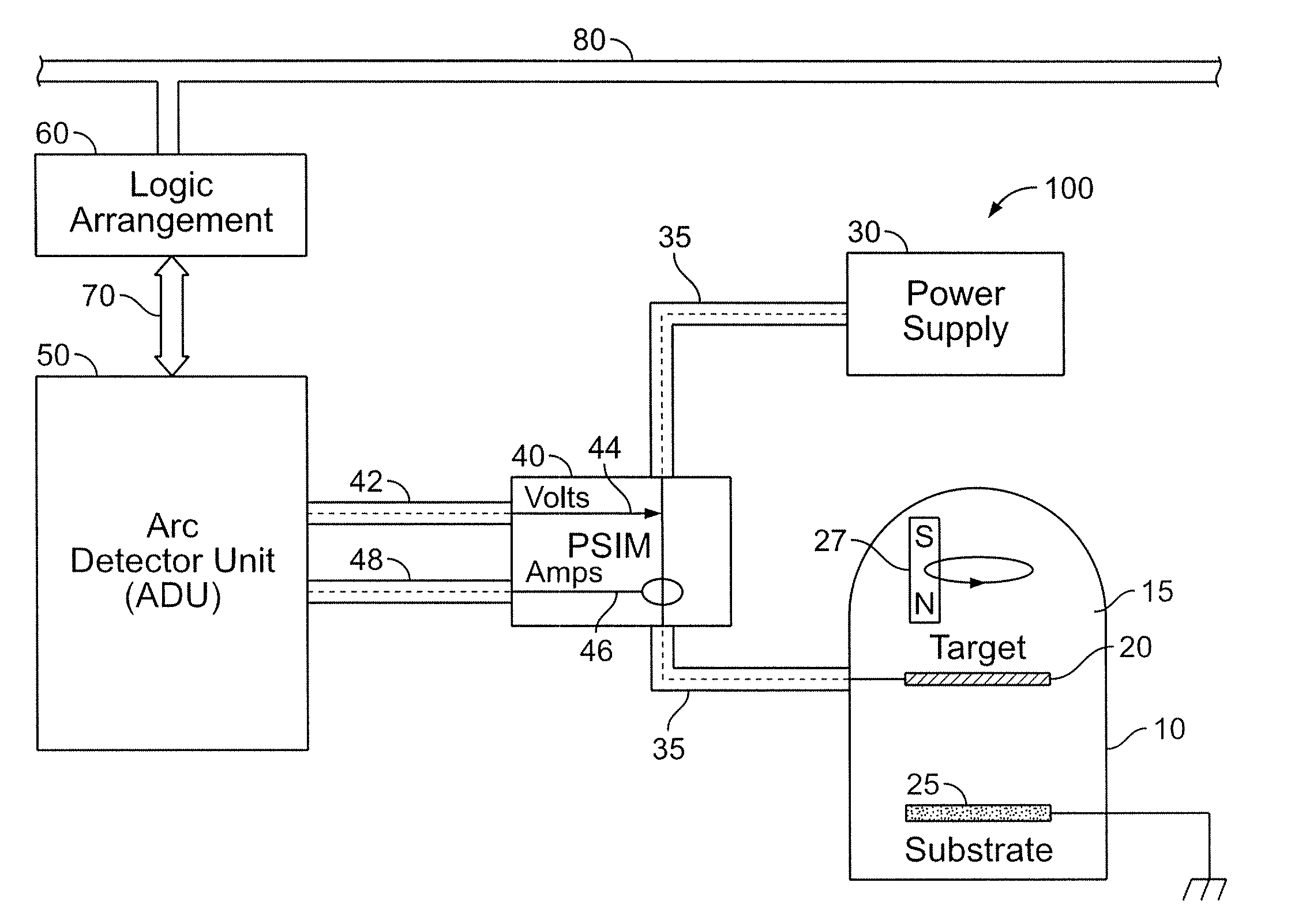
While determining the severity of cathode-anode or target arcing in a
physical vapor deposition chamber is a major concern, the occurrence of non-cathode arcs (NCAs) in the chamber is also problematic.
This presents a problem of how to indicate the occurrence of, or the potential of the occurrence of such NCAs.

