Method for generating nickel alloy self-aligned silicide

A self-aligned silicide, nickel alloy technology, applied in electrical components, semiconductor/solid-state device manufacturing, semiconductor devices, etc., to achieve the effect of improving performance, reducing production costs, and improving wafer yield

Active Publication Date: 2012-05-16
SEMICON MFG INT (SHANGHAI) CORP +1
View PDF5 Cites 0 Cited by
  • Summary
  • Abstract
  • Description
  • Claims
  • Application Information

AI Technical Summary

Problems solved by technology

[0010] In order to solve the problem that the prior art cannot effectively and economically reduce the corrosion effect of nickel in the nickel alloy salicide layer on the channel region of a CMOS device, the present invention provides a method for generating nickel alloy salicide method, said method comprising the following steps:

Method used


Image

  • Method for generating nickel alloy self-aligned silicide
  • Method for generating nickel alloy self-aligned silicide
  • Method for generating nickel alloy self-aligned silicide

Examples


Embodiment Construction

[0033] In the following description, numerous specific details are given in order to provide a more thorough understanding of the present invention. It will be apparent, however, to one skilled in the art that the present invention may be practiced without one or more of these details. In other examples, some technical features known in the art are not described in order to avoid confusion with the present invention.

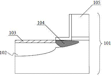
[0034] In order to thoroughly understand the present invention, detailed steps will be proposed in the following description, so as to illustrate how the present invention effectively and economically reduces the corrosion effect of nickel in the nickel alloy salicide layer on the channel region of the CMOS device, Improve the performance and wafer yield of CMOS devices. Obviously, the practice of the invention is not limited to specific details familiar to those skilled in the semiconductor arts. Preferred embodiments of the present invention are described in...


PUM


Abstract

The invention discloses a method for generating a nickel alloy self-aligned silicide, comprising the following steps of: providing to-be-produced wafers; selecting a first wafer and a second wafer from the to-be-produced wafers; generating a first nickel alloy metal film on the surface of the first wafer by a first nickel alloy target; generating a first nickel alloy self-aligned silicide on the first wafer by the first nickel alloy metal film; looking up the defect area on the first wafer; producing a second nickel alloy target; generating a second nickel alloy metal film on the surface of the second wafer by the second nickel alloy target; and generating a second nickel alloy self-aligned silicide on the second wafer by the second nickel alloy metal film. The erosion action on the channel region of a CMOS (complementary metal oxide semiconductor) apparatus by nickel in the nickel alloy self-aligned silicide can be efficiently reduced, the performance of the CMOS apparatus can be improved, and the yield of the wafer can be increased according to the method for generating the nickel alloy self-aligned silicide disclosed by the invention. The dosages of expensive constrained metals are efficiently reduced while the performance of the CMOS apparatus is improved via the method for generating the nickel alloy self-aligned silicide disclosed by the invention.

Description

technical field [0001] The invention relates to the field of semiconductor technology, in particular to a method for generating nickel alloy self-aligned silicide. Background technique [0002] In the semiconductor manufacturing process, the complementary metal oxide semiconductor (CMOS) device formed on the wafer is composed of a metal gate region, a silicon oxide gate dielectric region and a semiconductor silicon substrate. Wherein, the gate region is mostly made of polysilicon. However, the use of polysilicon leads to other problems, such as the degradation of device performance due to the high resistance of polysilicon. Therefore, the currently adopted method is to perform a silicide process after the device is formed to form a layer of metal silicide on the gate region and the source / drain region, thereby reducing the resistance of the device. [0003] The process of forming a layer of metal silicide on the gate region and source / drain region of a CMOS device is calle...

Claims


Application Information

Patent Timeline
Patent Type & Authority Applications(China)
IPC IPC(8): H01L21/28H01L21/283
Inventor 卢炯平聂佳相杨瑞鹏孔祥涛
Owner SEMICON MFG INT (SHANGHAI) CORP
Why Eureka
Try Eureka