

Method for improving bevel etching yield
A yield and slope technology, applied in the manufacturing of electrical components, circuits, semiconductor/solid-state devices, etc., can solve the problems of wafer yield reduction, backsplash, damage to the film layer, etc., and achieve wafer yield improvement and injection position. The effect of precision and improved wafer yield
- Summary
- Abstract
- Description
- Claims
- Application Information
AI Technical Summary
Problems solved by technology
Method used
Image

Examples
Embodiment Construction
[0024] The following will clearly and completely describe the technical solutions in specific embodiments of the present invention. Obviously, the described embodiments are only some of the embodiments of the present invention, not all of them. Based on the embodiments of the present invention, all other embodiments obtained by persons of ordinary skill in the art without making creative efforts belong to the protection scope of the present invention.
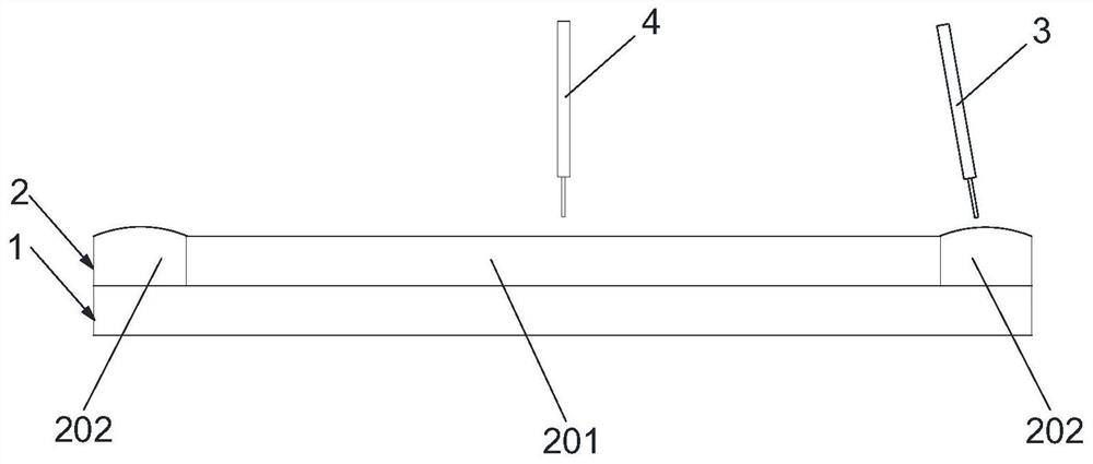
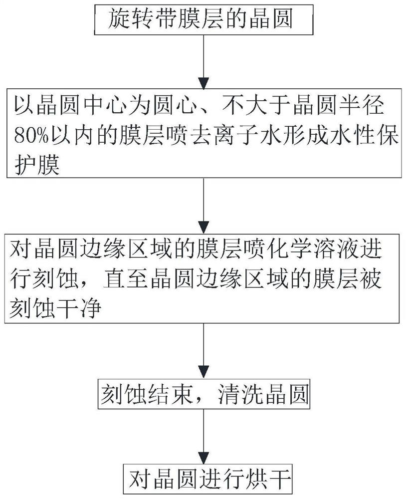
[0025] Embodiment 1 of the present invention provides a method for improving the yield rate of bevel etching. For the structure adopted, please refer to figure 1 , provide a wafer 1 with a film layer 2, the film layer 2 covers the upper surface of the entire wafer 1 in this embodiment, because the quality of some film layers in the edge region 202 of the wafer 1 is not good, it needs to be Etching is performed. The etching device in this embodiment is, for example, the first nozzle 3, the first nozzle 3 is located above the ed...
PUM
 Abstract
Description
Claims
Application Information