Supercharge Your Innovation With Domain-Expert AI Agents!

Light emitting element package

a technology packages, applied in the field can solve the problem of not cost-effective driving circuit of light emitting elements

Inactive Publication Date: 2013-09-17
ADVANCED OPTOELECTRONIC TECH INC
View PDF8 Cites 2 Cited by
  • Summary
  • Abstract
  • Description
  • Claims
  • Application Information

AI Technical Summary

Benefits of technology

This design allows for cost-effective and efficient operation of light emitting elements with an AC source by optimizing voltage management and heat dissipation, enhancing illumination efficiency and reliability.

Problems solved by technology

However, the drive circuit of the light emitting element is not cost-effective.

Method used


Image

  • Light emitting element package
  • Light emitting element package
  • Light emitting element package

Examples


first embodiment

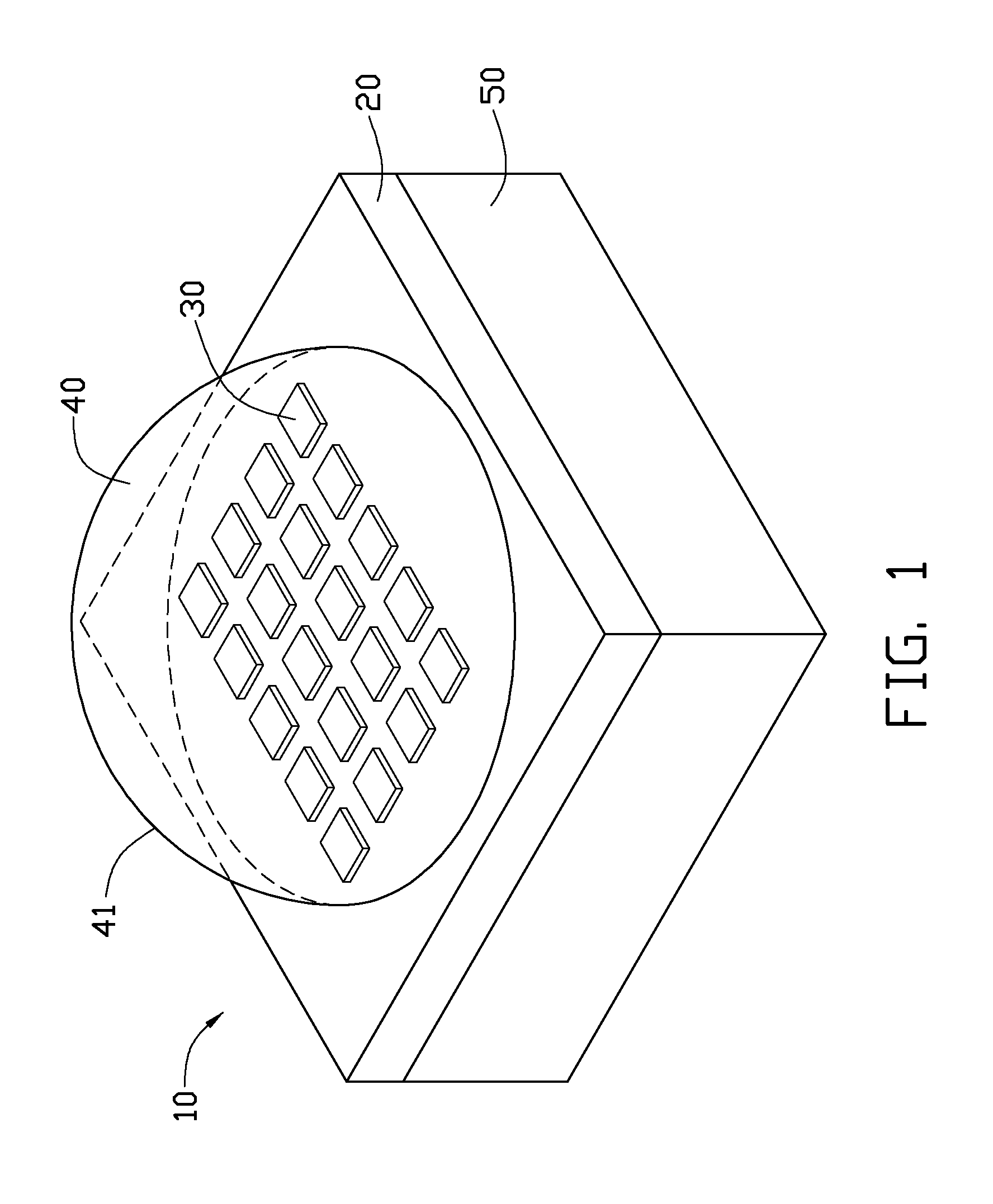
[0015]Referring to FIGS. 1-3, a light emitting element package 10 in accordance with the disclosure includes a substrate 20, a plurality of light emitting elements 30, an encapsulation member 40 and a heat dissipation substrate 50.

[0016]The light emitting elements 30 are mounted on one surface of the substrate 20. The encapsulation member 40 is configured for encapsulating the light emitting elements 30 on the substrate 20. The heat dissipation substrate 50 is mounted on a surface of the substrate 20 opposite to that on which the light emitting elements 30 are mounted. The heat dissipation substrate 50 is configured for dissipating heat generated by the light emitting elements 30.

[0017]Each of the light emitting elements 30 includes an extension substrate 31, a buffer layer 32 and a multi-layer epitaxial structure 33.

[0018]The extension substrate 31 can be sapphire, SiC, Si, GaAs, LiAlO2, MgO, ZnO, GaN, AN or InN.

[0019]The multi-layer epitaxial structure 33 includes an N-type semi-c...

third embodiment

[0030]Referring to FIG. 6, a light emitting element package 80 in accordance with the disclosure differs from the light emitting element package 70 only in that the light emitting element 80 includes only a third variable resister 806. The first light emitting element module 801 and the second light emitting element module 802 are connected in parallel. The third variable resister 806 is serially connected to the first light emitting element module 801 and the second light emitting element module 802.

fourth embodiment

[0031]Referring to FIG. 7, a light emitting element package 90 in accordance with the disclosure differs from light emitting element package 80 only in that the light emitting element package includes four light emitting element modules coupled to a fourth variable resister 906.


PUM


Abstract

A light emitting element package includes a substrate, at least two light emitting element modules and an encapsulation member. The substrate includes a circuit layer. The circuit layer includes a plurality of solder pads. The at least two light emitting element modules are mounted on the substrate. Each of the at least two light emitting element modules includes a plurality of light emitting elements. Each light emitting element of the at least two light emitting element modules is electrically coupled to neighboring light emitting element in serial through the solder pads. The at least two light emitting element modules are reversely arranged. The encapsulation member is configured to encapsulate the at least two light emitting element modules on the substrate.

Description

BACKGROUND[0001]1. Technical Field[0002]The disclosure relates generally to light emitting elements, and more particularly to a light emitting element powered by an AC source.[0003]2. Description of the Related Art[0004]Light emitting elements are often driven by a DC source. However, the drive circuit of the light emitting element is not cost-effective.[0005]Therefore, there is a need for improvement in the art.BRIEF DESCRIPTION OF THE DRAWINGS[0006]Many aspects of the embodiments can be better understood with references to the following drawings. The components in the drawings are not necessarily drawn to scale, the emphasis instead being placed upon clearly illustrating the principles of the embodiments. Moreover, in the drawings, like reference numerals designate corresponding parts throughout two views.[0007]FIG. 1 is an isometric view of a light emitting element package in accordance with a first embodiment of the disclosure.[0008]FIG. 2 is a cross-section of the light emittin...

Claims


Application Information

Patent Timeline
Patent Type & Authority Patents(United States)
IPC IPC(8): H01L29/18
CPCH01L25/0753H01L2224/16H01L33/62
Inventor HUANG, SHIH-CHENGTU, PO-MINYANG, SHUN-KUEIHUANG, CHIA-HUNG
Owner ADVANCED OPTOELECTRONIC TECH INC
Features
  • R&D
  • Intellectual Property
  • Life Sciences
  • Materials
  • Tech Scout
  • Unparalleled Data Quality
  • Higher Quality Content
  • 60% Fewer Hallucinations
Learn More