Optical navigation devices and associated methods

a technology of optical navigation and associated methods, applied in the field of optical navigation devices, can solve the problems of limiting the design of thin imaging devices, and reducing the size of the optical navigation device. , to achieve the effect of reducing the distortion of perspectiv

Active Publication Date: 2013-09-17
STMICROELECTRONICS (RES & DEV) LTD
View PDF7 Cites 1 Cited by
  • Summary
  • Abstract
  • Description
  • Claims
  • Application Information

AI Technical Summary

Benefits of technology

[0005]It is an object of the present invention to overcome at least some of the problems associated with the prior art as discussed above. It is a further object of the present invention to provide an optical navigation device having a thin sensor which may have less distortion than previous devices.
[0007]The present invention offers a number of benefits which may include a reduction to the perspective distortion and stray light shielding while maintaining a required thickness.

Problems solved by technology

As the computer devices become smaller, the various features of the computer devices may also become smaller.
However, with the smaller computer devices, minimizing the size of the optical navigation device can often be restrictive and problematic.
These have had some success but the design has generally not addressed all of the problems associated with thin imaging devices.
One such outstanding problem is associated with the positioning of the sensor.
However, this may then give rise to distortion such as perspective distortion, in the image generated at the sensor.
In addition, such de-centering of the sensor can cause problems with shielding the sensor from any stray light which enters the imaging surface.
These may require considerable space for the design which incorporates the ability to tilt and de-center the input lens to correct for any perspective effect.
However, the requirement of greater space may be undesirable in small-scale optical navigation devices.

Method used


Image

  • Optical navigation devices and associated methods
  • Optical navigation devices and associated methods
  • Optical navigation devices and associated methods

Examples


Embodiment Construction

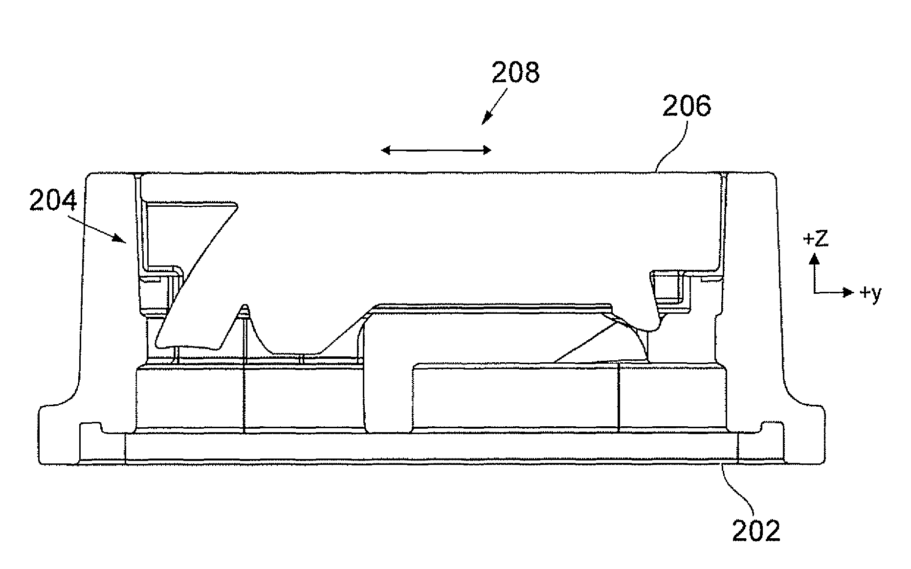
[0013]The present invention relates to an imaging device associated with an optical navigation device. The optical navigation device may be a mouse of small-scale which is intended to be operated via frustrated total internal reflection (F-TIR) to recognize the movement of a finger on an imaging surface. This type of mouse is herein referred to as a finger mouse.

[0014]FIG. 2 shows an example of a finger mouse 200 in accordance with an embodiment of the present invention. The finger mouse includes a base 202; an imaging device shown generally at 204; and an LED and sensor, both not shown. The top surface 206 of the imaging device 204 includes an imaging surface 208 which is positioned at a predetermined location on the surface 206. It will be appreciated that the position of the imaging surface will depend on the optical path or paths that light takes from the LED to the sensor. In addition, the position of the sensor relative to the imaging device will depend on the optics forming t...


PUM


Abstract

The imaging device has an imaging surface and a sensor, wherein the imaging surface is illuminated and reflects at least some of the illumination to the sensor to detect an image. The imaging device has a width and an optical path passing therethrough, wherein the optical path exhibits distortion as a result of the width of the device and the nature of the optical path. The imaging device includes an optical element which in use compensates for the distortion by generating a magnification profile across a tangential plane of the device at the sensor.

Description

FIELD OF THE INVENTION[0001]The present invention relates to optical navigation devices such as, for example, optical mice.BACKGROUND OF THE INVENTION[0002]Computer devices are becoming ever smaller and full computing functionality can be found on phones and smart phones and other personal digital assistants (FDA). As the computer devices become smaller, the various features of the computer devices may also become smaller. This includes a desire for smaller input systems for the user to enter inputs into the device. One such input system is an optical navigation device. Many computer devices, large and small, are equipped with optical navigation devices. However, with the smaller computer devices, minimizing the size of the optical navigation device can often be restrictive and problematic.[0003]A number of devices have been proposed which offer thin optical navigation devices. These have had some success but the design has generally not addressed all of the problems associated with...

Claims


Application Information

Patent Timeline
Patent Type & Authority Patents(United States)
IPC IPC(8): H04N5/225G06F3/033G01R21/00G06G7/24
CPCG01R21/00G06F3/0421G06G7/24G06F3/042
Inventor REIGNEAU, MATHIEU
Owner STMICROELECTRONICS (RES & DEV) LTD
Why Eureka
Try Eureka