Capacitive touch display panel
a capacitive touch display and display panel technology, applied in the field of can solve the problems of affecting the display performance of the capacitive touch display panel, affecting the thickness level, and increasing the manufacturing cost, so as to improve the light reflection problem, the effect of improving the light reflection problem and avoiding the increase of manufacturing cost and the thickness level
- Summary
- Abstract
- Description
- Claims
- Application Information
AI Technical Summary
Benefits of technology
Problems solved by technology
Method used
Image
Examples
first embodiment
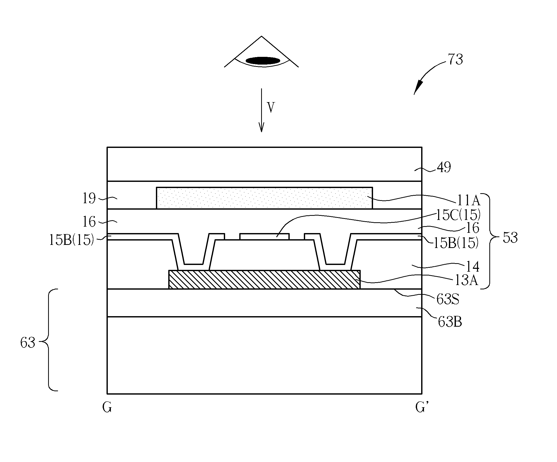
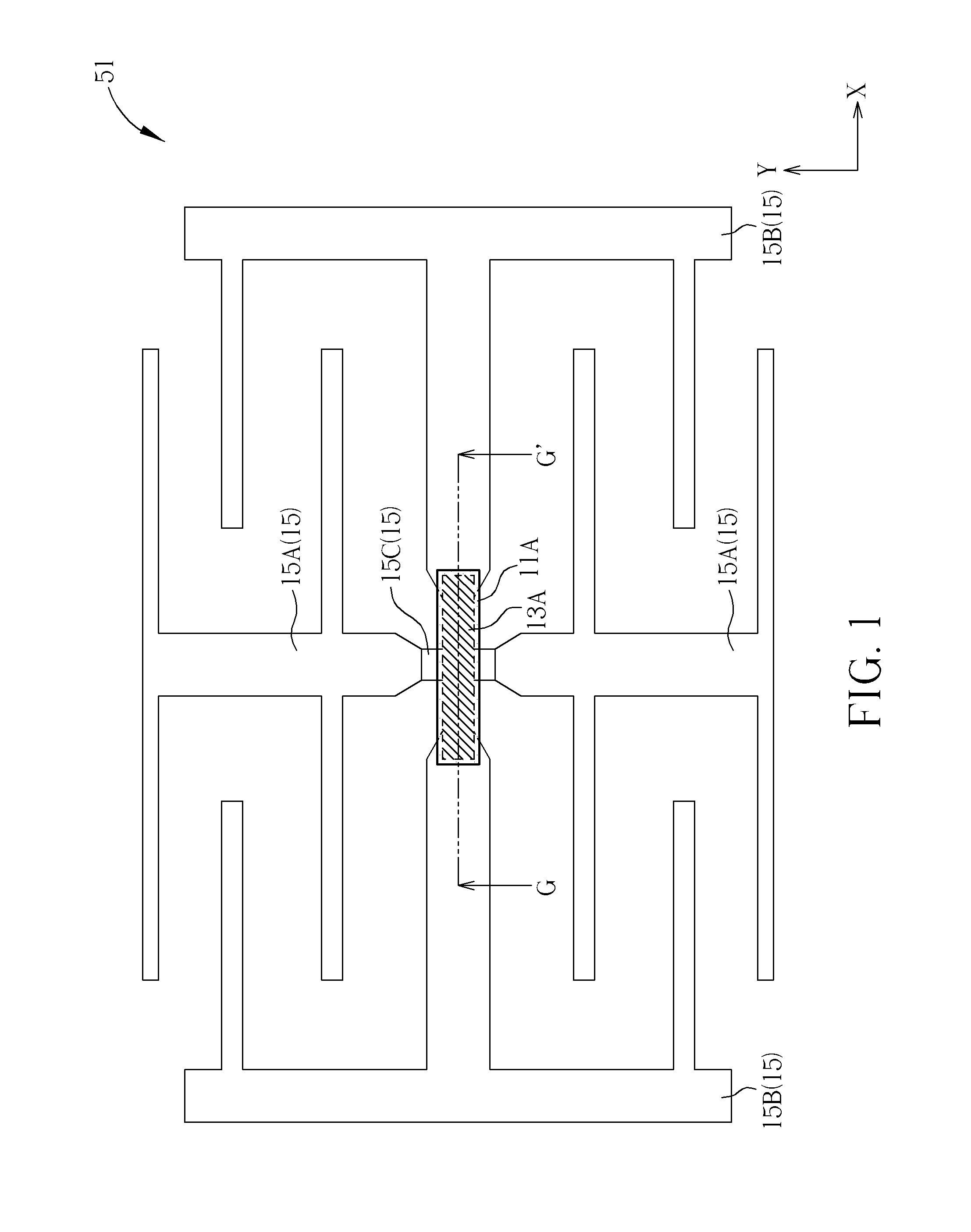
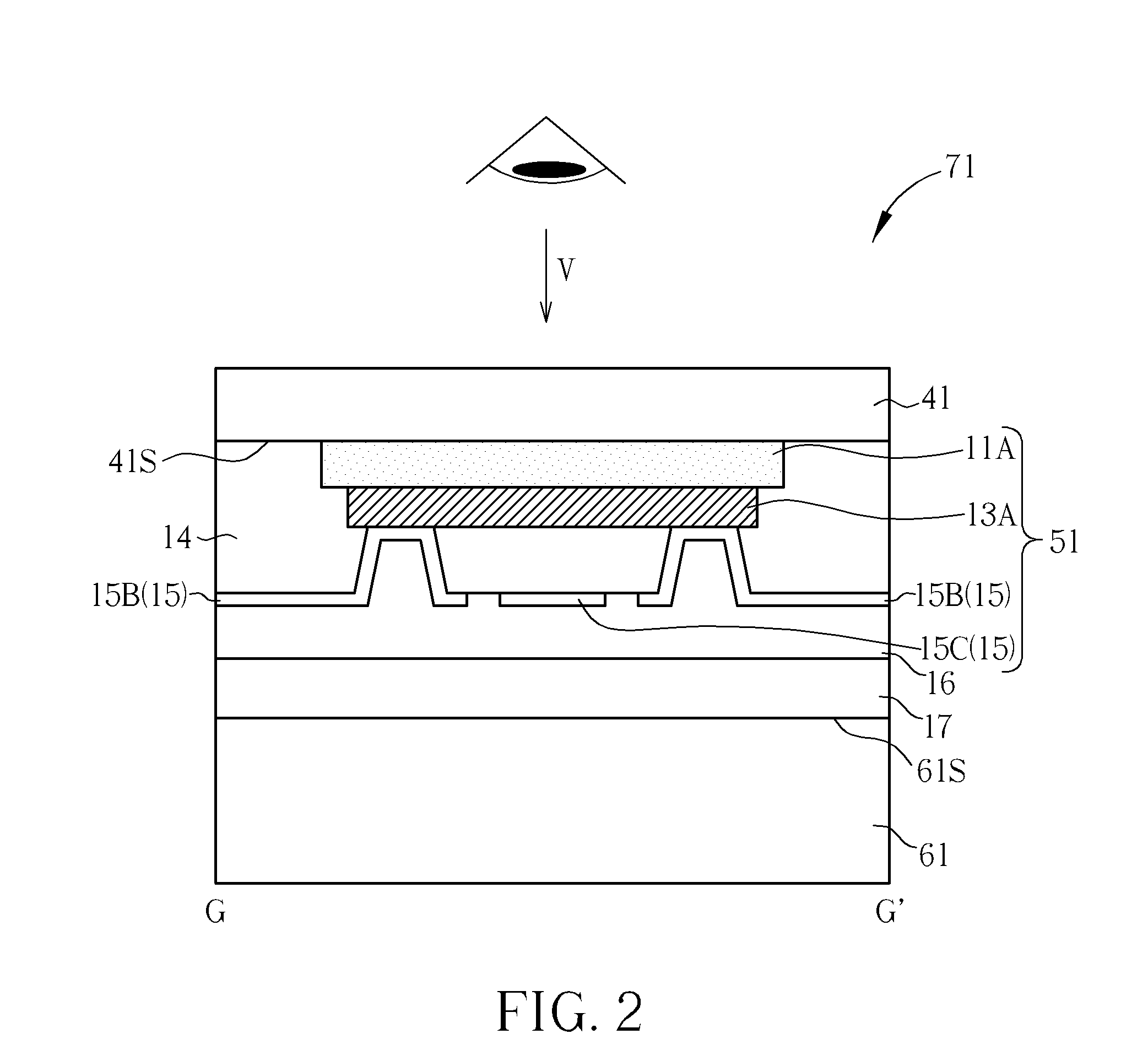
[0027]Please refer to FIG. 3, and refer to FIG. 1 together. FIG. 1 is a schematic diagram illustrating a top view of a capacitive touch display panel according to the second preferred embodiments of the present invention. FIG. 3 is a schematic diagram illustrating is a cross-sectional view of a capacitive touch display panel along a line G-G′ in FIG. 1 according to the second preferred embodiment of the present invention. As shown in FIG. 1 and FIG. 3, the capacitive touch display panel 72 includes a display panel 61, an outer substrate 41, a first insulating layer 14, a second insulating layer 12, a passivation layer 16, an adhesive layer 17, and a capacitive touch device 51. The display panel 61 has a display surface 61S, and the outer substrate 41 is disposed on the display surface 61S of the display panel 61. In this embodiment, the display panel 61 may include a liquid crystal display panel, an electroluminescent display panel, an electrophoretic display panel, or a plasma disp...
third embodiment
[0030]Please refer to FIG. 6, and refer to FIG. 4 together. FIG. 4 is a schematic diagram illustrating a top view of a capacitive touch display panel according to the fourth preferred embodiment of the present invention. FIG. 6 is a schematic diagram illustrating is a cross-sectional view of a capacitive touch display panel along a line G-G′ in FIG. 4 according to the fourth preferred embodiment of the present invention. As shown in FIG. 4 and FIG. 6, in this embodiment, the capacitive touch display panel 74 includes a display panel 63, a capacitive touch device 53, an auxiliary substrate 44, and a first adhesive layer 18. The display panel 63 includes an upper substrate 63B and a display surface 63S. In this embodiment, the display panel 63 may include a liquid crystal display panel, an electroluminescent display panel, an electrophoretic display panel, or a plasma display panel, but the present invention is not limited to this. The auxiliary substrate 44 is disposed between the di...
PUM
 Abstract
Description
Claims
Application Information


