Anneal to minimize leakage current in DRAM capacitor

a leakage current and capacitor technology, applied in the direction of capacitors, semiconductor devices, electrical equipment, etc., can solve the problems of high leakage current in the device, large leakage current in the capacitor stack implementing high-k dielectric materials, and prohibitively expensive noble metal systems when employed in a mass production contex

Inactive Publication Date: 2014-02-11
INTERMOLECULAR +1
View PDF11 Cites 9 Cited by
  • Summary
  • Abstract
  • Description
  • Claims
  • Application Information

AI Technical Summary

Problems solved by technology

The low band gap may lead to high leakage current in the device.
As a result, without the utilization of countervailing measures, capacitor stacks implementing high-k dielectric materials may experience large leakage currents.
The noble metal systems, however, are prohibitively expensive when employed in a mass production context.
Moreover, electrodes fabricated from noble metals often suffer from poor manufacturing qualities, such as surface roughness, poor adhesion, and form a contamination risk in the fab.
The use of crystalline conductive metal oxides as a second electrode in MIM DRAM capacitors has been difficult due to a number of problems.
Conductive metal oxides are sensitive to oxidation to oxygen-rich compounds that negatively impact their performance as an electrode material.
Reducing atmosphere anneal processes are not an option at this stage of the device manufacture because they would degrade the performance of the dielectric layer through the formation of oxygen vacancies.
However, it has been found that the patterning of the capacitor stack may damage the materials leading to high leakage current.

Method used


Image

  • Anneal to minimize leakage current in DRAM capacitor
  • Anneal to minimize leakage current in DRAM capacitor
  • Anneal to minimize leakage current in DRAM capacitor

Examples


Embodiment Construction

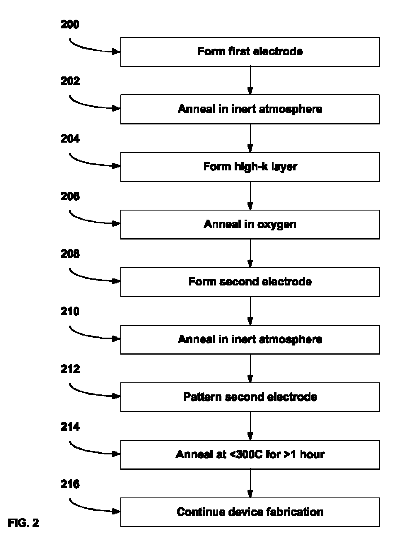
[0025]A detailed description of one or more embodiments is provided below along with accompanying figures. The detailed description is provided in connection with such embodiments, but is not limited to any particular example. The scope is limited only by the claims and numerous alternatives, modifications, and equivalents are encompassed. Numerous specific details are set forth in the following description in order to provide a thorough understanding. These details are provided for the purpose of example and the described techniques may be practiced according to the claims without some or all of these specific details. For the purpose of clarity, technical material that is known in the technical fields related to the embodiments has not been described in detail to avoid unnecessarily obscuring the description.

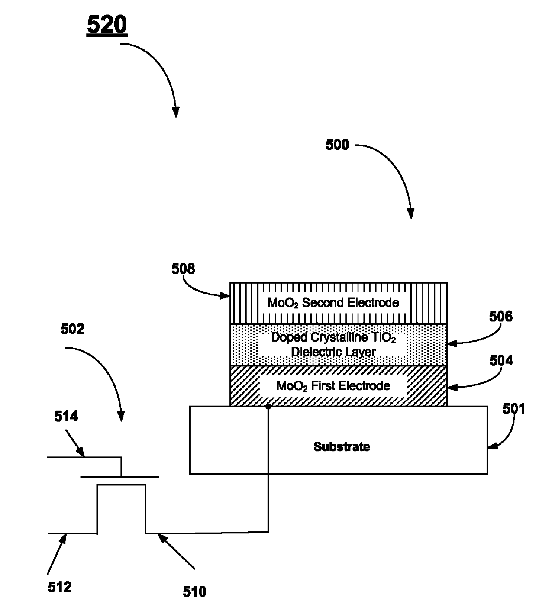
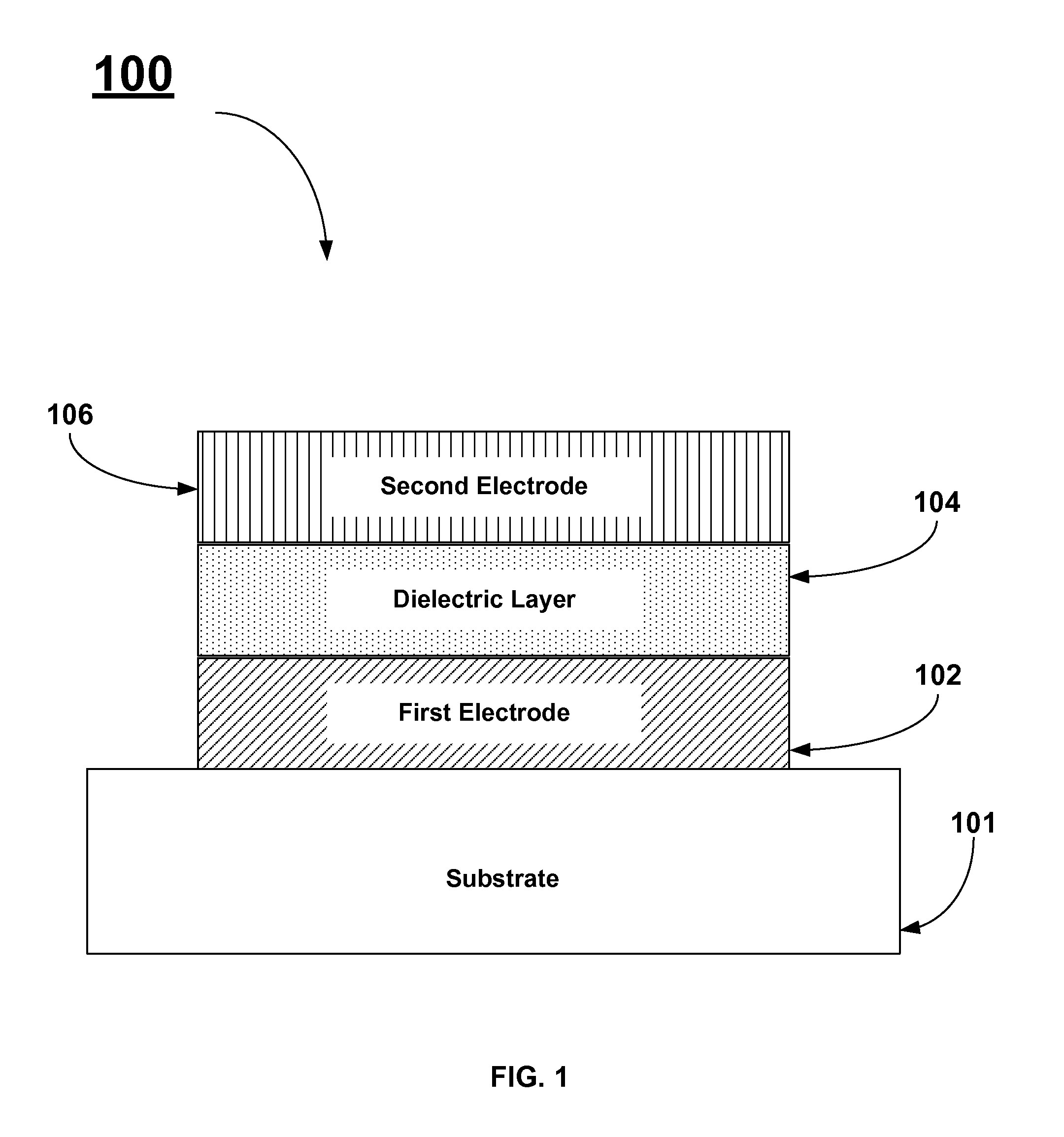
[0026]FIG. 1 illustrates a simplified cross-sectional view of a DRAM capacitor stack fabricated in accordance with some embodiments of the present invention. First electrode l...


PUM

PropertyMeasurementUnit
cell capacitanceaaaaaaaaaa
physical thicknessaaaaaaaaaa

Abstract

A method for forming a DRAM MIM capacitor stack comprises forming a first electrode layer, annealing the first electrode layer, forming a dielectric layer on the first electrode layer, annealing the dielectric layer, forming a second electrode layer on the dielectric layer, annealing the second electrode layer, patterning the capacitor stack, and annealing the capacitor stack for times greater than about 10 minutes, and advantageously greater than about 1 hour, at low temperatures (less than about 300 C) in an atmosphere containing less than about 25% oxygen and preferably less than about 10% oxygen.

Description

[0001]This document relates to the subject matter of a joint research agreement between Intermolecular, Inc. and Elpida Memory, Inc.FIELD OF THE INVENTION[0002]The present invention generally relates to the field of dynamic random access memory (DRAM), and more particularly to material processing for improved DRAM performance.BACKGROUND OF THE INVENTION[0003]Dynamic Random Access Memory utilizes capacitors to store bits of information within an integrated circuit. A capacitor is formed by placing a dielectric material between two electrodes formed from conductive materials. A capacitor's ability to hold electrical charge (i.e., capacitance) is a function of the surface area of the capacitor plates A, the distance between the capacitor plates d (i.e. the physical thickness of the dielectric layer), and the relative dielectric constant or k-value of the dielectric material. The capacitance is given by:[0004]C=κ⁢⁢ɛo⁢Ad(Eqn.⁢1)where ∈0 represents the vacuum permittivity.[0005]The dielec...

Claims


Application Information

Patent Timeline
Patent Type & Authority Patents(United States)
IPC IPC(8): H01L21/20
CPCH01L28/40H01L28/60
Inventor DEWEERD, WIMODE, HIROYUKI
Owner INTERMOLECULAR
Why Eureka
Try Eureka