Methods for UV-assisted conformal film deposition

Inactive Publication Date: 2014-02-11
NOVELLUS SYSTEMS
View PDF181 Cites 337 Cited by
  • Summary
  • Abstract
  • Description
  • Claims
  • Application Information

AI Technical Summary

Problems solved by technology

One issue with SiN films is the relatively high temperatures used to form the films, for example, in Front End of Line (FEOL) applications, SiN films are typically deposited by chemical vapor deposition (CVD) in a reactor at greater than 750° C. using dichlorosilane and ammonia.

Method used


Image

  • Methods for UV-assisted conformal film deposition
  • Methods for UV-assisted conformal film deposition
  • Methods for UV-assisted conformal film deposition

Examples


examples

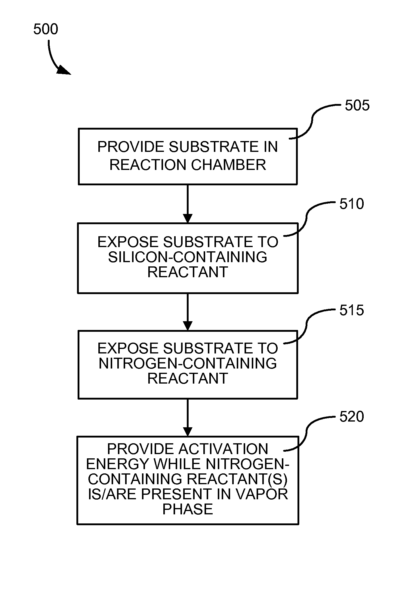
[0119]Bis(dimethylamono)dimethyl silane and an N-reactant were reacted to form Si-containing films by UV and remote plasma-assisted methods according to embodiments described herein. A UV cure apparatus with four stations each including a UV lamp was used. The process sequences were as follows:

[0120]UV ALD: Bis(dimethylamono)dimethyl silane exposure on Stations 1 & 3 (UV lamps OFF), UV with NH3 exposure on Stations 2 & 4. Sequence: Bis(dimethylamono)dimethyl silane exposure→purge→purge→index to next station→UV in NH3→purge→index to next station. Typical bis(dimethylamono)dimethyl exposure time was 20 s, with 2 mL / min of flow with 1 slm carrier (Ar) on Stations 1 & 3. The wafer was allowed to soak for 60 s in Stations 1 & 3. The film contained SiN with C likely to be present based on width of the SiNC peak. Significant amounts of both N—H and Si—H were present.

[0121]Remote plasma ALD: Bis(dimethylamono)dimethyl silane exposure on Stations 3 & 4, remote plasma with NH3 (+Ar) exposure ...


PUM

PropertyMeasurementUnit
temperaturesaaaaaaaaaa
temperatureaaaaaaaaaa

Abstract

Described are methods of making silicon nitride (SiN) materials and other silicon-containing films, including carbon-containing and / or oxygen-containing films such as SiCN (also referred to as SiNC), SiON and SiONC films, on substrates. According to various embodiments, the methods involve electromagnetic radiation-assisted activation of one or more reactants. In certain embodiments, for example, the methods involve ultraviolet (UV) activation of vapor phase amine coreactants. The methods can be used to deposit silicon-containing films, including SiN and SiCN films, at temperatures below about 400° C.

Description

[0001]This application claims benefit under 35 USC §119(e) of U.S. Provisional Application No. 61 / 591,230, titled “METHODS FOR UV-ASSISTED CONFORMAL FILM DEPOSITION,” filed Jan. 26, 2012, which is incorporated by reference herein. This application also claims priority, as a continuation-in-part under 35 USC §120, to U.S. patent application Ser. No. 13 / 084,305, filed Apr. 11, 2011, and titled “SILICON NITRIDE FILMS AND METHODS.”INTRODUCTION[0002]1. Field[0003]The present disclosure relates generally to formation of silicon-containing materials, including SiN, SiCN and SiC materials on substrates. More particularly, the disclosure relates to formation of silicon-containing films on semiconductor substrates.[0004]2. Background[0005]Silicon nitride (SiN) thin films have unique physical, chemical and mechanical properties and thus are used in a variety of applications, particularly semiconductor devices, for example in diffusion barriers, gate insulators, sidewall spacers, encapsulation ...

Claims


Application Information

Patent Timeline
Patent Type & Authority Patents(United States)
IPC IPC(8): H01L21/469H01L21/31
CPCH01L21/0228H01L21/0214H01L21/02219C23C16/325H01L21/02211H01L21/0217H01L21/02167H01L21/02277C23C16/45536H01L21/02274H01L21/02126
Inventor LAVOIE, ADRIENVARADARAJAN, BHADRIHENRI, JONHAUSMANN, DENNIS
Owner NOVELLUS SYSTEMS
Why Eureka
Try Eureka