Developing device and image forming apparatus including the same
a technology of developing device and image forming apparatus, which is applied in the direction of electrographic process apparatus, instruments, optics, etc., can solve the problems of unstable toner charge amount, image defect, and inability to obtain stable image density, so as to reduce image density and suppress uneven toner density
- Summary
- Abstract
- Description
- Claims
- Application Information
AI Technical Summary
Benefits of technology
Problems solved by technology
Method used
Image
Examples
first embodiment
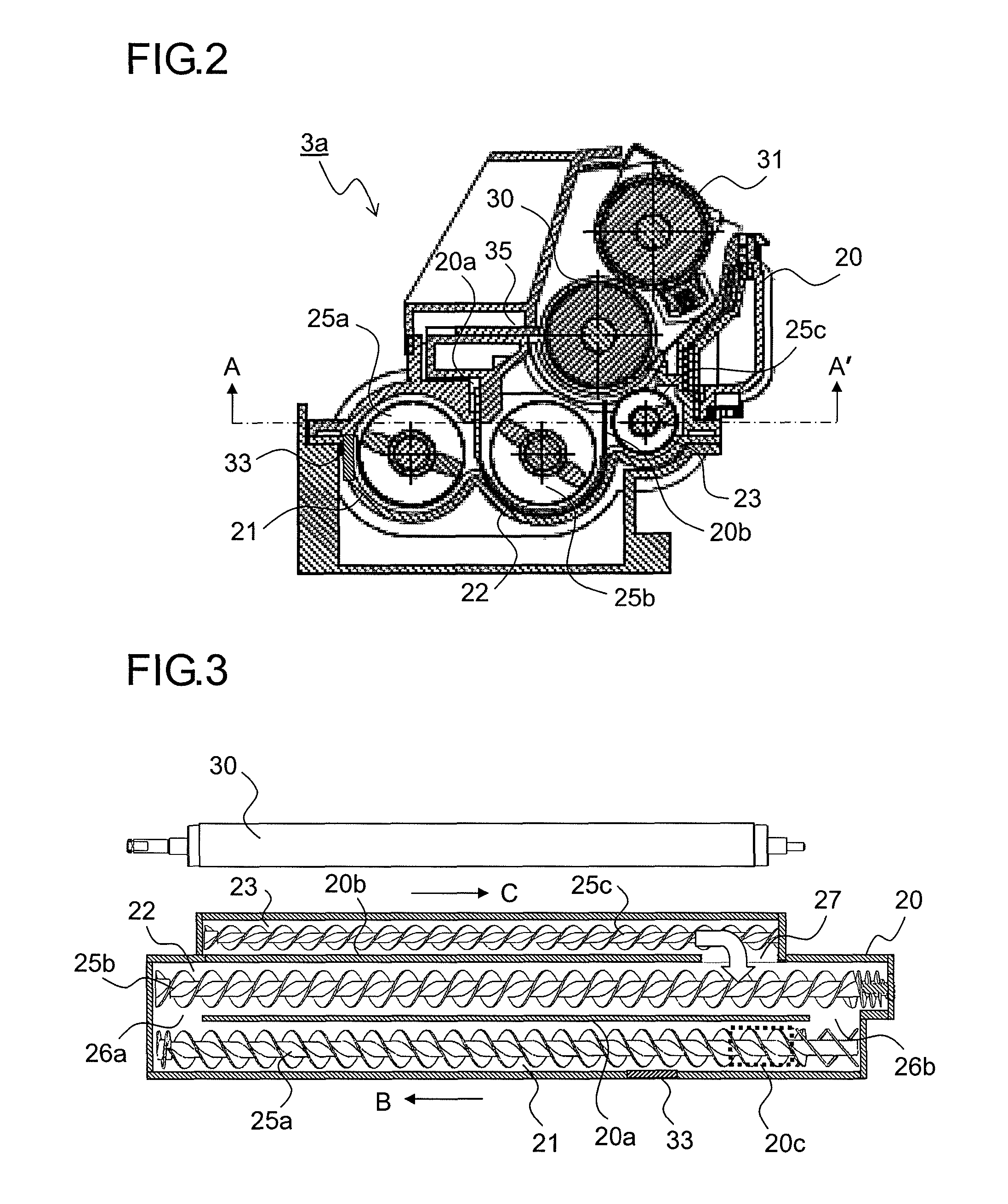
[0072]Therefore, a distance by which the developer within the collecting-transport chamber 23 is transported after being merged into the developer within the supplying-transport chamber 22 up to the toner replenishing port 20c is longer than in the first embodiment in which the developer within the collecting-transport chamber 23 is merged into the developer within the supplying-transport chamber 22 only from the communication portion 27. As a result, the developer within the supplying-transport chamber 22 is replenished with the toner after being sufficiently stirred and made uniform, and hence it is possible to further stabilize the toner density within the developer.
[0073]Further, the developer is gradually returned to the supplying-transport chamber 22 from not only the communication portion 27 but also the wide-range region on the upstream side thereof, which facilitates the control of the developer amount within the supplying-transport chamber 22 and can improve stability of a...
second embodiment
[0075]FIGS. 9A and 9B are perspective views schematically illustrating other structural examples of the collecting-transport chamber of the developing device according to the FIG. 9A illustrates structure in which a plurality of opening portions 40 are provided in the partition wall 20b, and FIG. 9B illustrates structure in which the partition wall 20b is gradually lowered from an upstream side in the transporting direction of the developer toward the downstream side.
[0076]The width of the region through which the developer is returned from the collecting-transport chamber 23 to the supplying-transport chamber 22 and the returning amount of the developer can be adjusted by changing the shape, size, number, and layout of the opening portions 40 provided in the partition wall 20b in the case of the structure of FIG. 9A and by changing the inclination of a top surface of the partition wall 20b in the case of the structure of FIG. 9B.
[0077]Next described is a developing device accordin...
third embodiment
[0086]FIG. 12 is a sectional side view illustrating another structural example of the developing device according to the present invention, and FIG. 13 is a sectional plan view (sectional view from the arrows AA′ of FIG. 12) illustrating another structural example of the developing device. In FIG. 12, the transporting speed of the collecting-transport screw 25c is set slower than that of the supplying-transport screw 25b in the developing device of a two-component development method which is not provided with the developing roller 31 on which the toner thin layer is formed and performs the development by bringing the magnetic brush formed on the magnetic roller 30 into direct contact with the photosensitive drum 1a.
[0087]Further, as illustrated in FIG. 13, the communication portion 27 is provided in substantially the same position as the second developer passage 26b in terms of the transporting direction of the developer (direction indicated by the arrow C).
[0088]Also in the develo...
PUM
 Abstract
Description
Claims
Application Information


