Supercharge Your Innovation With Domain-Expert AI Agents!

Method for forming resistive switching memory elements

a technology memory elements, which is applied in the field of semiconductor memories, can solve the problems of increasing the size requirements, high voltage peripheral transistors adding to the cost and complexity of resistive switching memory, and nano-laminates not providing adequate electronic defect density

Inactive Publication Date: 2014-08-12
INTERMOLECULAR
View PDF10 Cites 4 Cited by
  • Summary
  • Abstract
  • Description
  • Claims
  • Application Information

AI Technical Summary

Problems solved by technology

EPROM, also known as flash memory, uses an architecture that is inadequate in its access, erase and write times for the rapidly increasing operational speed requirements and rapidly decreasing size requirements of electronic devices.
High voltage peripheral transistors add to the cost and complexity of the resistive switching memory.
The nano-laminates do not provide adequate electronic defect density for ideal electron transport through the metal oxide / insulator.

Method used


Image

  • Method for forming resistive switching memory elements
  • Method for forming resistive switching memory elements
  • Method for forming resistive switching memory elements

Examples


Embodiment Construction

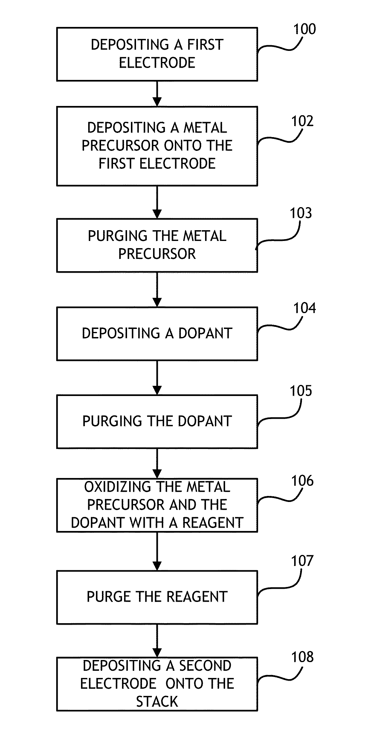
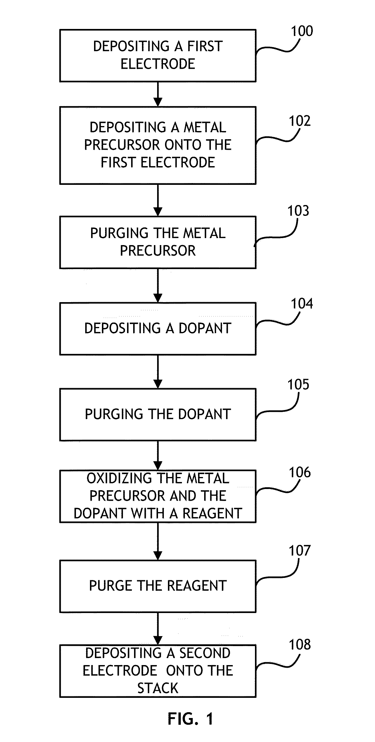
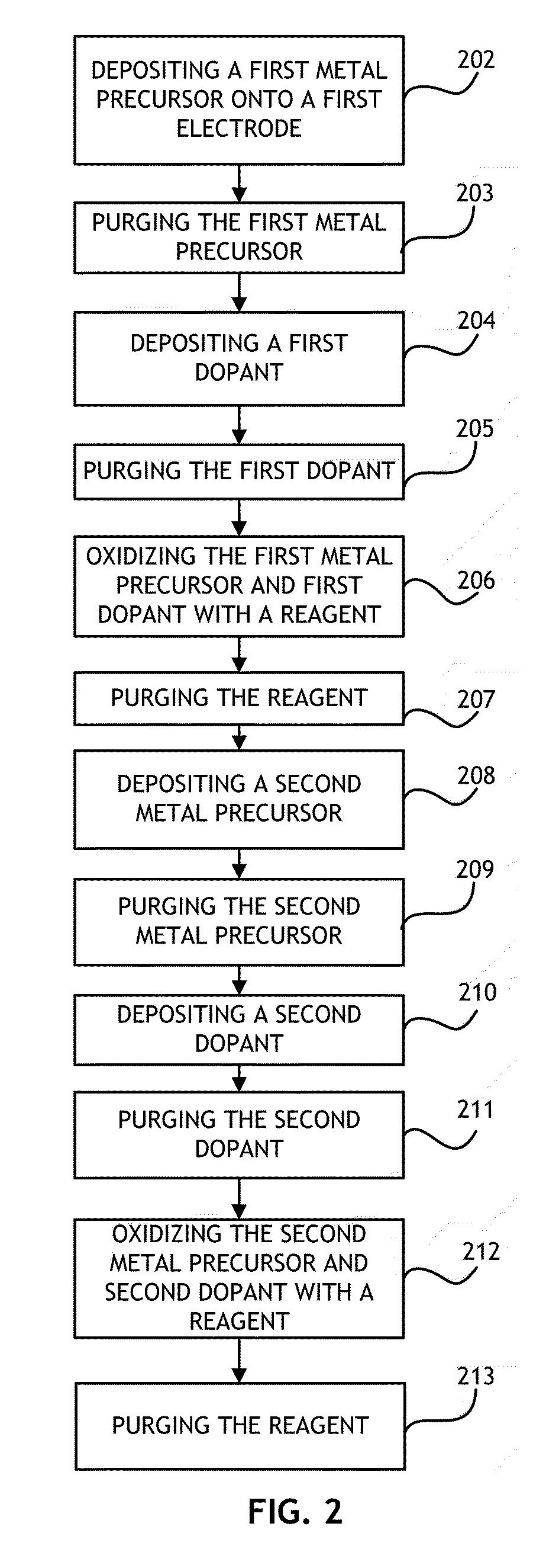
[0017]The present invention relates to methods for producing Resistive Random Access Memory (RRAM) resistive switching elements having a reduced forming and switching voltages. Embodiments of the present invention may reduce forming and set voltages by doping the insulator with a dopant that enhances the insulator's ability to form conductive pathways. The dopant may be uniformly distributed throughout the insulator or the dopant may be uniformly distributed in a region near the interface between the insulator and an electrode.

[0018]RRAM resistive switching elements with reduced forming and set voltages are useful because RRAM resistive switching elements with reduced forming and set voltages require lower voltage peripheral transistors. The scope of the invention is limited only by the claims; numerous alternatives, modifications and equivalents are encompassed. For the purpose of clarity, technical material that is known in the technical fields related to the embodiments has not b...


PUM

PropertyMeasurementUnit
concentrationaaaaaaaaaa
chamber pressureaaaaaaaaaa
switching voltagesaaaaaaaaaa

Abstract

Methods for producing RRAM resistive switching elements having reduced forming voltage include doping to create oxygen deficiencies in the dielectric film. Oxygen deficiencies in a dielectric film promote formation of conductive pathways.

Description

FIELD OF THE INVENTION[0001]The present invention relates generally to semiconductor memories and more particularly a method for forming a resistive switching memory element with reduced forming and switching voltages.BACKGROUND OF THE INVENTION[0002]All but the simplest of electronic devices utilize nonvolatile memories. When an electronic device must retain information during and after being placed in an unpowered state, nonvolatile memories must be provided. Several types of nonvolatile memories are known in the art. Nonvolatile memories may be portable, auxiliary, or integrated in a circuit or as a component in both general and embedded computer systems. Most generally, nonvolatile memories are found in digital cameras, cellular telephones, music players, and as the key component in portable memory devices such as USB based flash drives.[0003]Nonvolatile memory is often formed using electrically-erasable programmable read only memory (EPROM) technology. EPROM, also known as flas...

Claims


Application Information

Patent Timeline
Patent Type & Authority Patents(United States)
IPC IPC(8): H01L21/00H01L21/16
CPCH01L45/04H01L45/146H01L45/1616H01L45/1633H01L45/1658H10N70/20H10N70/826H10N70/023H10N70/8833H10N70/021H10N70/028H10N70/046
Inventor TONG, JINHONGHIGUCHI, RANDALLHASHIM, IMRANGOPAL, VIDYUT
Owner INTERMOLECULAR
Features
  • R&D
  • Intellectual Property
  • Life Sciences
  • Materials
  • Tech Scout
  • Unparalleled Data Quality
  • Higher Quality Content
  • 60% Fewer Hallucinations
Learn More