LED substrate structure, LED unit and lighting module having the same

a technology of led substrate and led unit, which is applied in the direction of semiconductor/solid-state device manufacturing, electrical apparatus, semiconductor devices, etc., can solve the problems of reduced adhesion ability of soldering materials, increased difficulty in soldering, so as to facilitate the climbing of soldering materials, reduce the length of cutting segments, and improve the fixing strength between led substrate structure and carrier boards

Active Publication Date: 2014-08-12
LITE ON ELECTRONICS (GUANGZHOU) LTD +1
View PDF7 Cites 0 Cited by
  • Summary
  • Abstract
  • Description
  • Claims
  • Application Information

AI Technical Summary

Benefits of technology

[0007]One object of the instant disclosure is providing a LED substrate structure, a LED unit that utilizes the LED substrate structure, and a lighting module incorporating the LED unit. The LED substrate structure has an improved conducting portion capable of reducing the length of a cutting segment where burr may be formed. Further, the conducting portion has oblique sides to facilitate a soldering material climbing from a carrier board. Thus, the fixing strength between the LED substrate structure and the carrier board is improved.
[0008]By reducing the length of the first cutting segment, the problem of the climbing resistance resulted from the burr of the first cutting segment may be solved. On the other hand, an expansion region adjacent to the first cutting segment is formed as a sector-like area so that the soldering material may climb upon the conducting portion more easily and efficiently.

Problems solved by technology

The burr along the edge of the metal portion (where the width thereof is the widest) creates a long and unsmooth segment that makes it difficult for soldering.
In other words, the burrs formed on the metal portion of the LED unit along the cutting path may reduce the soldering material's adhesion ability.
Particularly, under common low temperature soldering process conditions in which soldering material still retain high viscosity and thus exhibits poor flowability / wettability, poor soldering may occur more often.
As a result, production yield would be negatively affected.
Due to the difference in material characteristics between the plastic packaging material and the metallic die-bonding area of the substrate, the contact interface therebetween may exhibit inadequate bonding strength.
As a result, the packaging material may spill out through the interface or the soldering material may undesirably permeate into the LED packaging material.
In addition, moisture from the surrounding environment may enter into the LED through the plastic-metal boding interface to contaminate the LED die.
As a result, the reliability and the stability of the traditional LED unit suffer.

Method used


Image

  • LED substrate structure, LED unit and lighting module having the same
  • LED substrate structure, LED unit and lighting module having the same
  • LED substrate structure, LED unit and lighting module having the same

Examples


Embodiment Construction

[0023]The embodiment of the instant disclosure will now be described hereinafter and identical or similar elements in the various figures are designated with the same reference numerals.

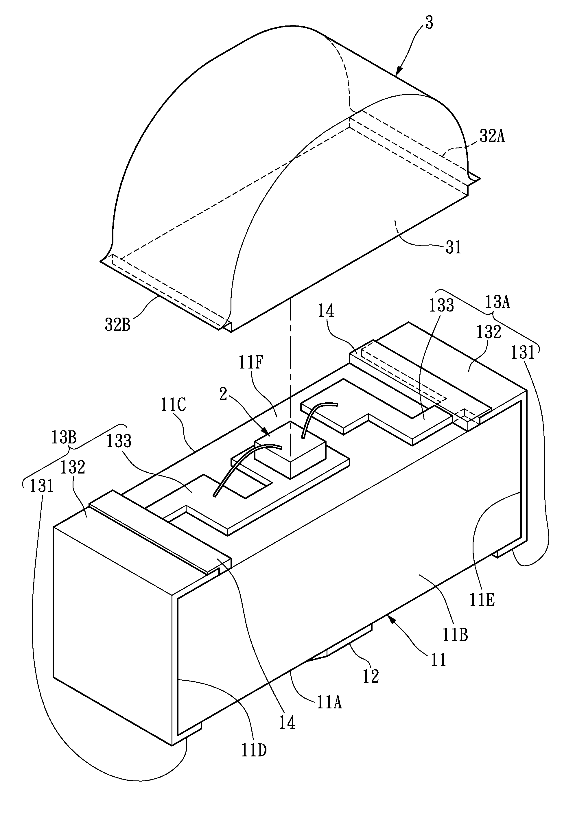
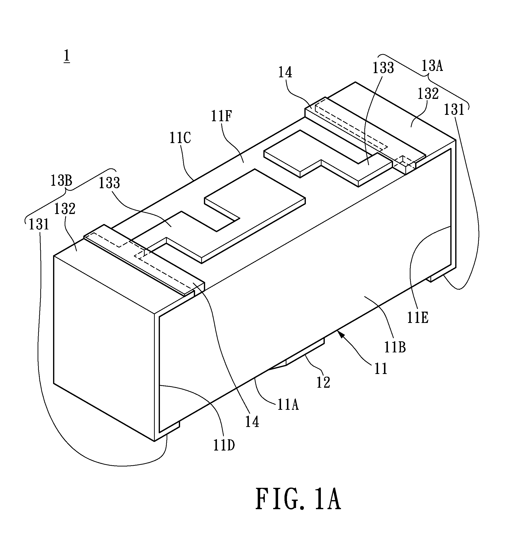
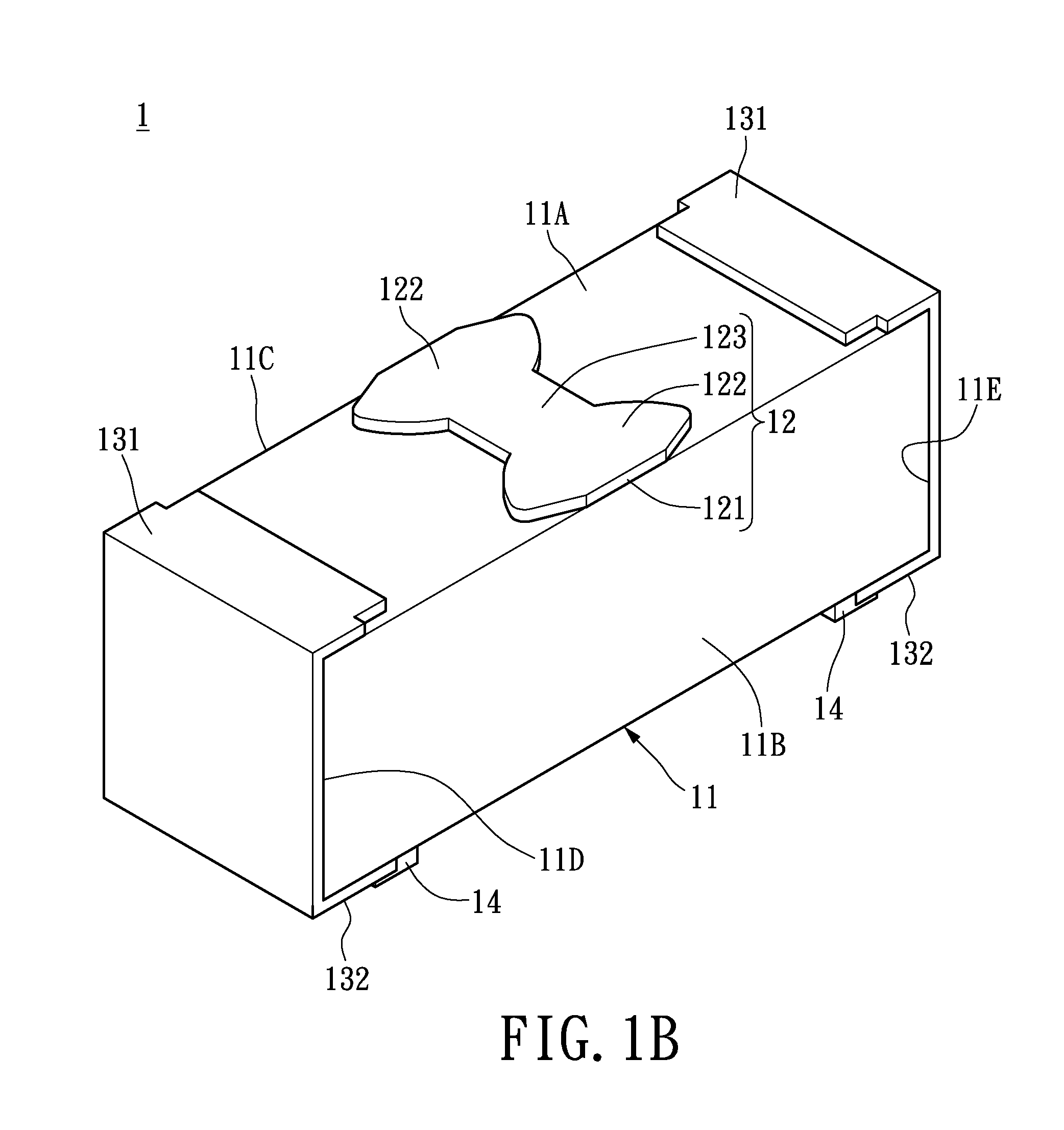
[0024]Please refer to FIGS. 1A and 1B, which shows a top isometric view and a bottom isometric view of an exemplary LED substrate structure in accordance with the instant disclosure. The instant disclosure provides a LED substrate structure 1 which comprises a substrate 11 having a conducting portion 12 formed thereon. The conducting portion 12 has an expansion region 122 with modified width variation so that the soldering materials may more easily climb up on the expansion region 122, thus achieving better connection strength with a carrier board after soldering.

[0025]Please refer to FIG. 2, which shows an overhead view of the bottom surface of a LED substrate structure 1 in accordance with the instant disclosure. The substrate 11 is preferably a rectangular parallelepiped upon dicing / sawing from a ...


PUM


Abstract

An LED substrate structure has a substrate and a conducting portion. The substrate has a bottom surface and two opposite first lateral surfaces connected with the bottom surface. The bottom surface has the conducting portion formed thereon, and the conducting portion has a first cutting segment located on a contact border defined between one of the two first lateral surfaces and the bottom surface. The conducting portion further has an expansion region connected with the first cutting segment. The length of the first cutting segment is shorter than any segment taken on the expansion region parallel thereto.

Description

BACKGROUND OF THE INVENTION[0001]1. Field of the Invention[0002]The present invention relates to a substrate structure, a light emitting device (LED) unit having such substrate structure, and a light source module utilizing such LED unit. Particularly, the present invention relates to a LED substrate structure, a LED unit and a lighting module having the same.[0003]2. Description of Related Art[0004]LEDs can be disposed on a printed circuit board (PCB) through surface-mount technique (SMT) as a surface-mount device. Depending on the illumination style / arrangement of the LED die, the surface mounted LEDs can be further classified into a side-view type and a top-view type.[0005]In the conventional LED unit assembling process, at least one LED die is mounted on a substrate and then encapsulated by a packaging material to form a LED unit. In the side-view type LED unit, the LED unit is mounted side-way on the PCB in such a way that a lateral surface adjacent to a rear metal portion of t...

Claims


Application Information

Patent Timeline
Patent Type & Authority Patents(United States)
IPC IPC(8): H01L33/62H01L33/48
CPCH01L33/62H01L33/486H01L2224/48091H01L25/0753H01L33/54H01L2224/48227H01L2924/00014
Inventor LEE, HOU-TEYING, TSUNG-KANGCHU, CHIA-HUNGYU, SHIH-PO
Owner LITE ON ELECTRONICS (GUANGZHOU) LTD
Why Eureka
Try Eureka