Process for cleaning wafers
a technology of wafers and cleaning processes, applied in the direction of chemistry apparatus and processes, cleaning using liquids, detergent compositions, etc., can solve the problems of shortening the time involved in surface treatment, and achieve the effects of reducing interaction, reducing surface energy of recessed portions, and increasing contact angl
- Summary
- Abstract
- Description
- Claims
- Application Information
AI Technical Summary
Benefits of technology
Problems solved by technology
Method used
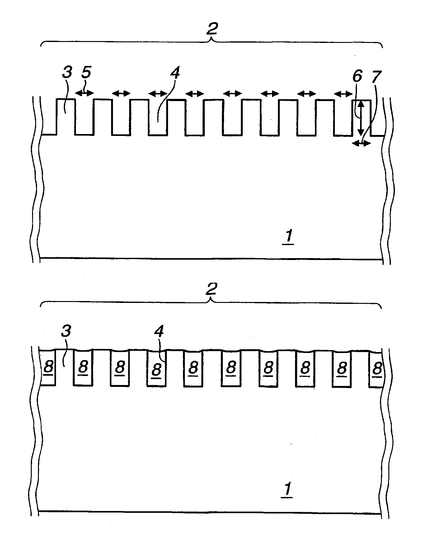
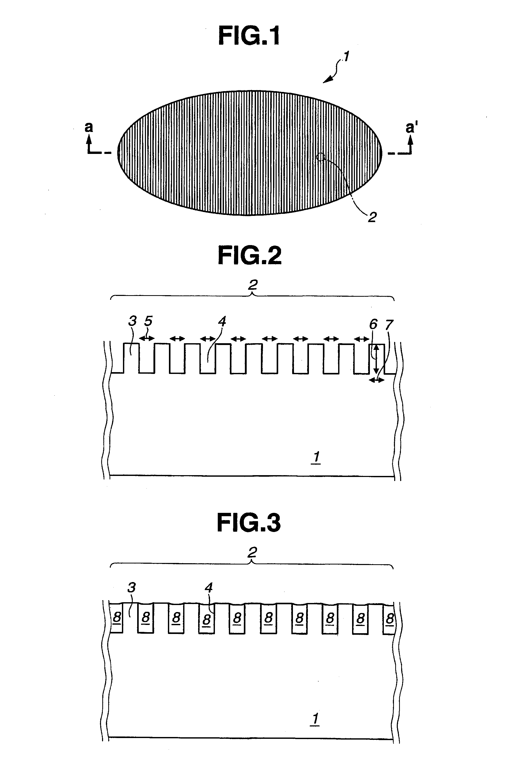
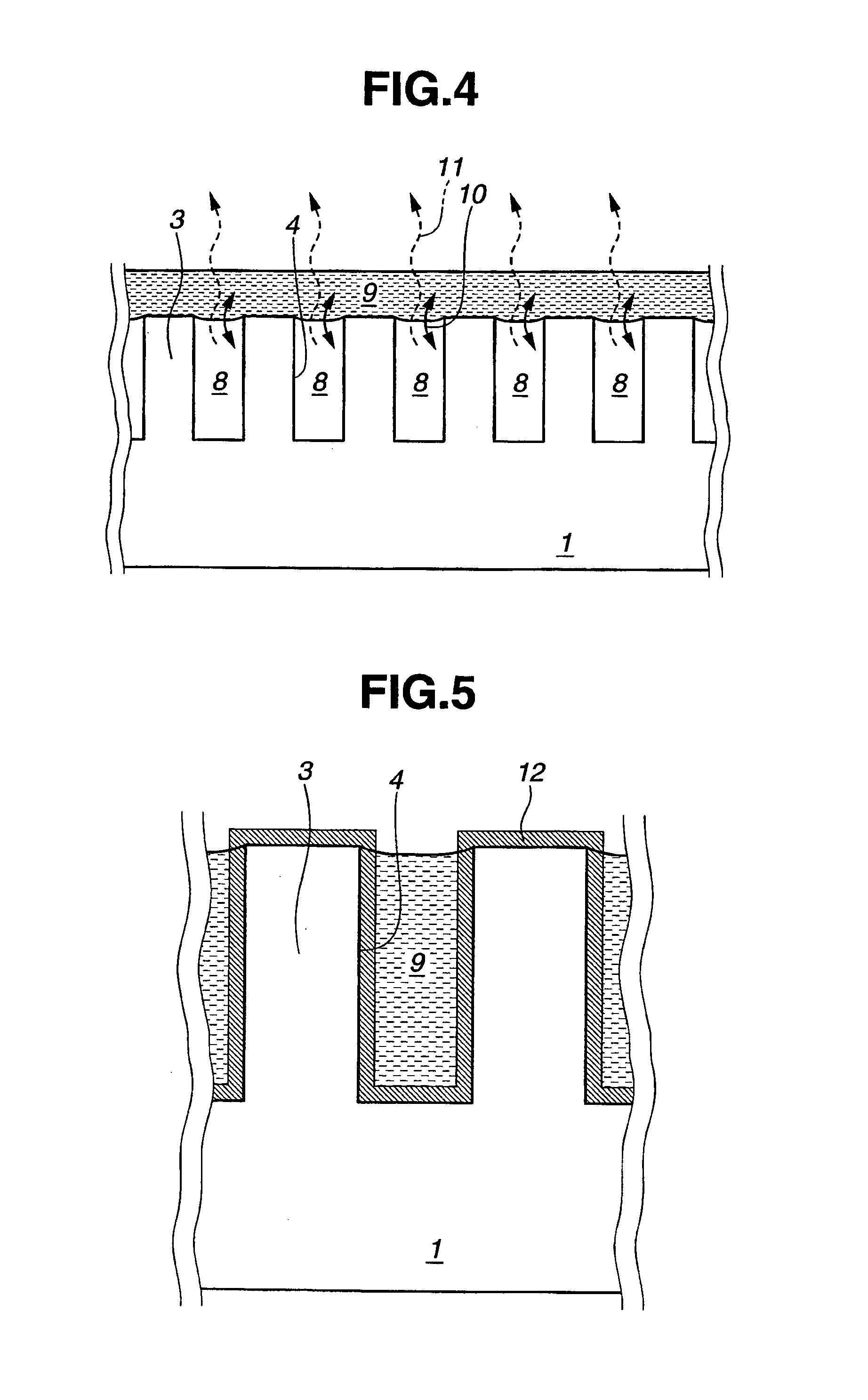
Image

Examples
example 1-1
(1) Cleaning of Wafer, Using Cleaning Liquid
[0213]A wafer having a smooth thermal oxide film (a silicon-based wafer formed having a thermal oxide film of 1 μm thickness on its surface) was immersed in 1 mass % hydrogen fluoride aqueous solution at room temperature for 2 minutes. Thereafter, the wafer was immersed in pure water for 1 minute, and then in 2-propanol (iPA; 82° C. Boiling Point) for 1 minute. Accordingly, a cleaning liquid retained on the surface of the wafer after cleaning is iPA.
(2) Preparation of Water-Repellent Liquid Chemical
[0214]In the present example, 5 g of hexamethyldisilazane [(H3O3Si—NH—Si(CH3)3] as a silicon compound A, 0.1 g of trimethylsilyl trifluoroactate [(CH3)3Si—OC(O)CF3] as a silicon compound B, and 94.9 g of propylene glycol monomethyl ether acetate (PGMEA) as an organic solvent were mixed thereby obtaining a water-repellent liquid chemical. Incidentally, a component the amount of which is the largest in mass ratio among components of the water-repe...
examples 1-2 to 1-10
Comparative Examples 1-1 to 1-5
[0219]Upon modifying those used in Example 1-1 (i.e., the temperature of the water-repellent liquid chemical, the cleaning liquid used before a water-repellency-imparting treatment, and the solvent for the water-repellent liquid chemical), the wafer having a thermal oxide film was subjected to the surface treatment and then evaluated. The results are shown in Table 1. By the way, DEGEEA means diethylene glycol monoethyl ether acetate. A component the amount of which is the largest in mass ratio among components of the water-repellent liquid chemical using the solvent is DEGEEA and its boiling point is 218° C. Furthermore, PGDA means propylene glycol diacetate; a component the amount of which is the largest in mass ratio among components of the water-repellent liquid chemical using the solvent is PGDA and its boiling point is 190° C. Additionally, PGMEA / DEE means a solvent obtained by mixing PGMEA and diethyl ether (DEE; 35° C. Boiling Point) at a mass ...
example 2-1
[0220]The procedure of Example 1-1 was repeated with the exception that 5 g of hexamethyldisilazane [(H3C)3Si—NH—Si(CH3)3] as a silicon compound D, 0.1 g of trifluoroacetic anhydride [{CF3C(O)}2O] as an acid D and 94.9 g of PGMEA as an organic solvent were mixed and reacted thereby obtaining a water-repellent liquid chemical containing trimethylsilyl trifluoroacetate as the silicon compound B, hexamethyldisilazane as the silicon compound A, and PGMEA as the organic solvent. Incidentally, a component the amount of which is the largest in mass ratio among components of the water-repellent liquid chemical is PGMEA and its boiling point is 146° C. Hexamethyldisilazane contained in the water-repellent liquid chemical of the present Example is the silicon compound D not consumed by the reaction for obtaining the silicon compound B, and this component functions as the silicon compound A. The result is shown in Table 2.
[0221]
TABLE 2Cleaning Liquid used before WaterTemperatureRequired Time f...
PUM
| Property | Measurement | Unit |
|---|---|---|
| boiling point | aaaaa | aaaaa |
| temperature | aaaaa | aaaaa |
| temperature | aaaaa | aaaaa |
Abstract
Description
Claims
Application Information
 - R&D Engineer
- R&D Manager
- IP Professional
- Industry Leading Data Capabilities
- Powerful AI technology
- Patent DNA Extraction
Browse by: Latest US Patents, China's latest patents, Technical Efficacy Thesaurus, Application Domain, Technology Topic.
© 2024 PatSnap. All rights reserved.Legal|Privacy policy|Modern Slavery Act Transparency Statement|Sitemap