Chip for optical analysis

a technology of optical analysis and chips, applied in the direction of positive displacement liquid engines, laboratory glasswares, instruments, etc., can solve the problems of inability to perform pretreatment operations, inability to eliminate impurities, inability to perform simple measurement, etc., to achieve accurate liquid analysis, change in baseline, and high sensitivity

Active Publication Date: 2014-10-14
NIPPON TELEGRAPH & TELEPHONE CORP
View PDF11 Cites 1 Cited by
  • Summary
  • Abstract
  • Description
  • Claims
  • Application Information

AI Technical Summary

Benefits of technology

[0011]An object of the present invention is to provide a chip for optical analysis which can very easily and conveniently determine how a measurement object is contained in a liquid to be measured by preparing a reference sample from the liquid to be measured as a reference.
[0012]Furthermore, another object of the present invention is to provide a chip for optical analysis which can prepare a reference sample in which a substance to be measured is free and selectively detect a measurement object in the real sample only by introducing a real sample into the chip for analysis.
[0013]Furthermore, another object of the present invention is to provide a chip for analysis which can suppress a signal noise generated from a difference in adsorption or accumulation of impurities to a measurement region and a reference region in a measurement method for detecting a substance to be measured based on an interaction between a probe molecule immobilized on a substrate and the substance to be measured, for example, a measurement method using a total reflection optical system. Even when a liquid sample to be measured by the chip for analysis of the present invention contains many impurities, measurement using a total reflection optical system can be achieved with higher sensitivity and higher precision.
[0028]The chip for optical analysis according to the present invention can prepare a reference sample in which a substance to be measured is free only by introducing a liquid sample containing the substance to be measured into the sample introduction section, and can measure the reference sample and a real sample containing this substance to be measured. Furthermore, according to the present invention, DNA, RNA, ions, amino acids, and peptides can be easily sensed with high sensitivity.
[0029]Since the chip for optical analysis of the present invention is provided with the means for allowing a liquid to be measured to reach the observation section from the branching section through the first passage earlier than reaching the observation section from the branching section through the second passage, the reference sample that is passed through a filter reaches the observation section first. Therefore, even when a simple surface plasmon resonance measurement device is used, a signal serving as the reference of a measured value can be first obtained, and then the liquid to be measured that is passed through the second passage reached the observation section, resulting in an accurate analysis of the liquid to be measured. In the chip for optical analysis of the present invention, the observation section can be provided with a measurement region and a reference region. With such a structure, a reference sample can be prepared only by supplying the liquid to be measured from the introduction port into the first passage, and a measurement object can be detected and quantified based on an interaction between a material having molecular selectivity immobilized on the measurement region and the measurement object.
[0030]According to the present invention, a change in the baseline that occurs at the time of measurement of a real sample containing many impurities can be minimized, and a small amount of a substance to be measured in a sample containing many impurities can be detected.

Problems solved by technology

However, when this reference sample is prepared, a complex pretreatment operation may be required, and such necessity of a pretreatment operation is not desirable in on-site or simple measurement.
In consideration of on-site measurement, such elimination treatment of impurities is not desirable either.
Such measurement by a total reflection optical system in which a probe molecule is immobilized on a substrate beforehand as described above suffers from a problem that many impurities are adsorbed or accumulated in a space on a substrate in which a measurement region is provided.
Therefore, a problem arises that, even if a difference between the reference region and the measurement region is deducted, effects of impurities cannot be eliminated, a baseline for measurement changes, and the baseline changes more greatly than a signal to be detected.
In a simple device without moving parts, however, it is impossible to detect a resonance angle in a condition where a sample is not introduced, and a signal cannot be obtained.
On the contrary, a problem arises that, even if a device has a mobile detection system, rapid measurement is impossible because the detection operation requires time.

Method used


Image

  • Chip for optical analysis
  • Chip for optical analysis
  • Chip for optical analysis

Examples


example 1

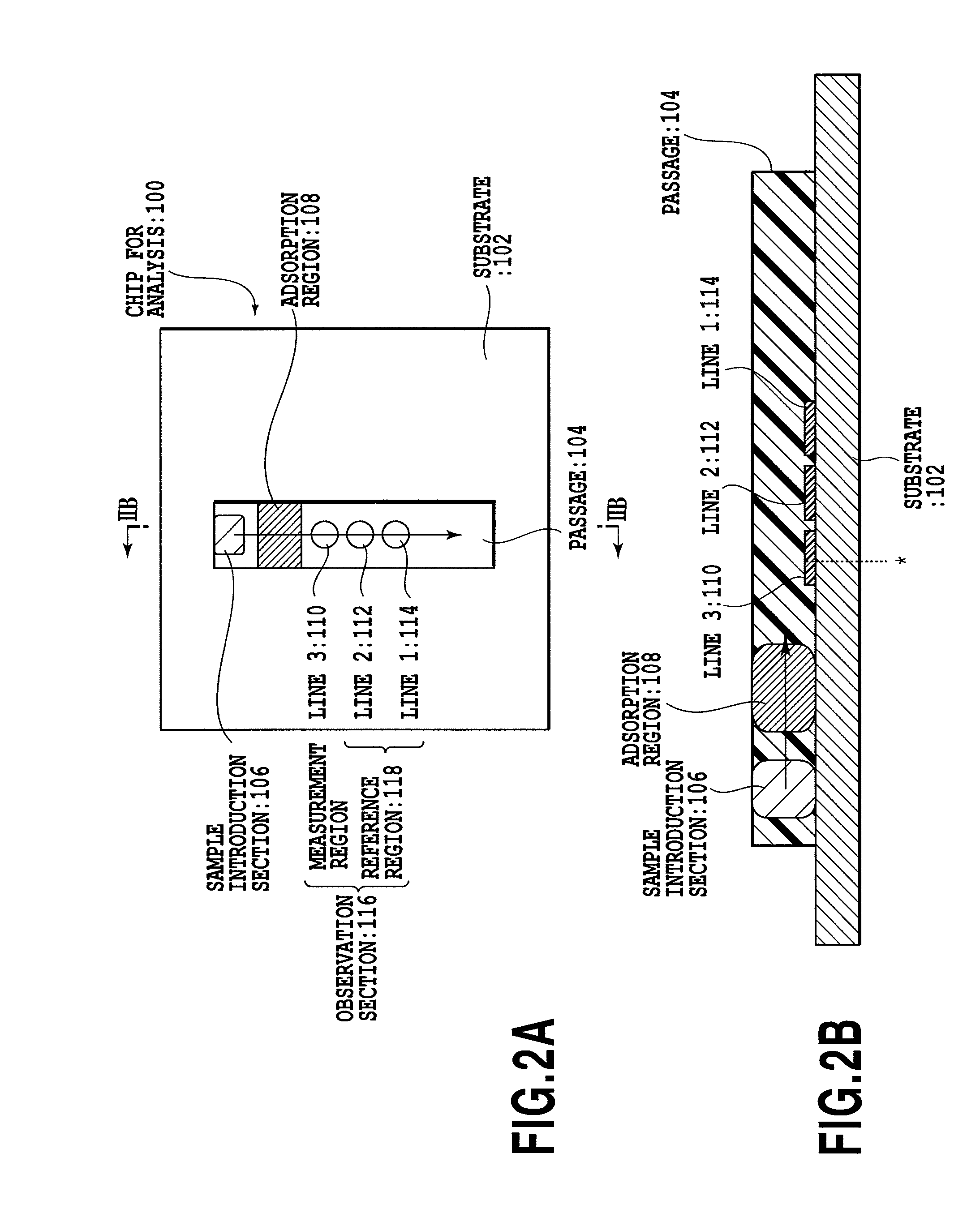
[0152]This example shows a chip for optical analysis for a passage without a bypass passage as shown in FIGS. 2A and 2B, for which a protein A adsorbent is used as an adsorbent.

[0153]Cellulose acetate was dissolved in an organic solvent to prepare a cellulose acetate solution. A gold thin film (thickness 50 nm) was formed on a BK7 glass substrate by vapor-deposition. A resist membrane or a tape was applied onto this gold thin film, and a pattern in which a portion of the gold thin film corresponding to a passage was exposed was formed. The patterned gold / glass substrate was mounted on a spin coater, the cellulose acetate solution prepared beforehand was added dropwise to the substrate, then the substrate was rotated, and the organic solvent was evaporated to form a white membrane-form passage. Subsequently, a buffer solution of protein A was prepared and added dropwise to an adsorption region of the passage, and protein A was adsorbed to the passage to form the adsorption region. Th...

example 2

[0159]This example shows a chip for optical analysis for a passage without a bypass passage as shown in FIGS. 2A and 2B, for which a modified dextran microparticle adsorbent is used as an adsorbent.

[0160]A cellulose acetate solution obtained by dissolving cellulose acetate in an organic solvent and modified dextran microparticles (obtained from the microparticlation of methacrylate-modified dextran by radical polymerization) (diameter 15 to 30 μm) were mixed to prepare a cellulose acetate-dextran microparticle mixture solution. A gold thin film (thickness 50 nm) was formed on a BK7 glass substrate by vapor-deposition. A resist membrane or a tape was applied onto this gold thin film to form a pattern in which a portion of the gold thin film corresponding to a passage was exposed. At this time, an adsorption region of the passage on the metal thin film was prevented from being exposed, and the cellulose acetate solution was prevented from being deposited on the adsorption region. Subs...

example 3

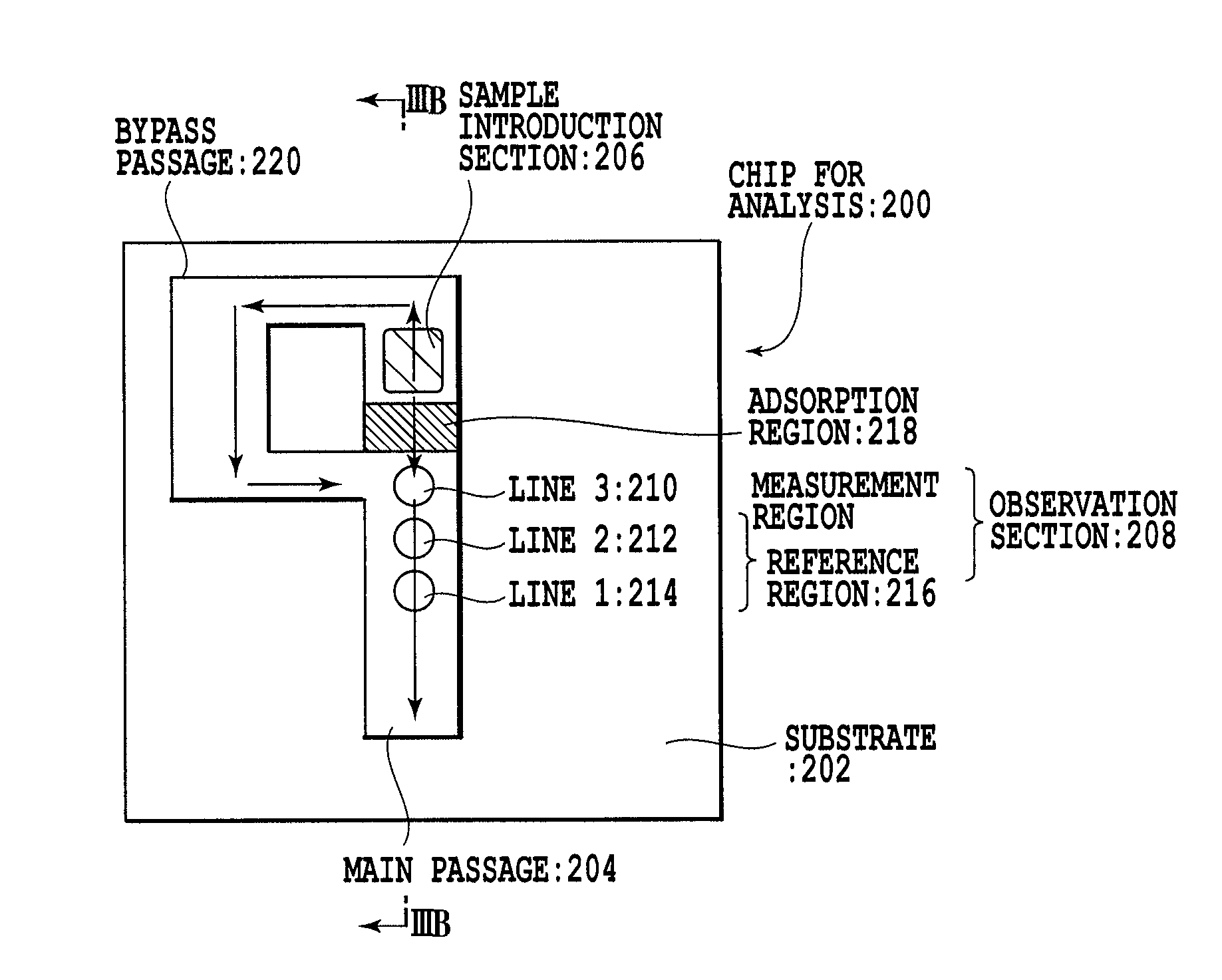
[0166]This example is a chip for optical analysis with a passage having a bypass passage as shown in FIGS. 3A and 3B using a protein A adsorbent as an adsorbent.

[0167]Cellulose acetate was dissolved in an organic solvent to prepare a cellulose acetate solution. A gold thin film (thickness 50 nm) was formed on a BK7 glass substrate by vapor-deposition. A resist membrane or a tape was applied onto this gold thin film, and a pattern in which portions of the gold thin film corresponding to the main passage and the bypass passage were exposed was formed. The patterned gold / glass substrate was mounted on a spin coater, the previously prepared cellulose acetate solution was added dropwise, then the substrate was rotated, and the organic solvent was evaporated to form white membrane-form main passage and bypass passage. Subsequently, a buffer solution of protein A was prepared and added dropwise onto an adsorption region of the passage, and protein A was adsorbed to the passage to form the ...


PUM

PropertyMeasurementUnit
thicknessaaaaaaaaaa
thicknessaaaaaaaaaa
thicknessaaaaaaaaaa

Abstract

The present invention relates to a chip for optical analysis. In particular, the present invention relates to an optical sensor handling a liquid sample, which is a chip for analysis that can be used for selectively measuring a biologically-relevant substance or a chemical substance such as an environmental pollutant or a health affecting substance in a liquid to be measured. The chip for optical analysis of the present invention is characterized in that (1) an adsorption region (filter region) is provided between a sample introduction section and the observation section in a passage of the chip for analysis, (2) a bypass passage is provided in the passage (main passage) of the chip for analysis, and a time lag is generated between samples passed through the main passage and passed through a bypass passage, and (3) a measurement region and a reference region are provided in the observation section of the chip for analysis. In the present invention, the aspects (1) to (3) can be achieved individually or two or more thereof can be combined.

Description

TECHNICAL FIELD[0001]The present invention relates to a chip for optical analysis. In particular, the present invention relates to a chip for analysis, which can be used for an optical sensor for handling a liquid sample that selectively measures chemical substances such as a biologically-relevant substance or an environmental pollutant or a health affecting substance in a liquid to be measured. The chip for analysis of the present invention can use a substance having molecular selectivity. Furthermore, the chip for analysis of the present invention measures a real sample containing impurities, with higher measurement sensitivity and higher precision in measurement. The chip for analysis of the present invention is intended for a simpler operation in measurement and higher sensitivity and higher precision in measurement.BACKGROUND ART[0002]The method for measuring a chemical substance in a liquid sample include for example electric and optical measurement methods in which a substanc...

Claims


Application Information

Patent Timeline
Patent Type & Authority Patents(United States)
IPC IPC(8): C12M1/40G01N21/01B01L3/00G01N21/05G01N21/27G01N21/41G01N21/55
CPCG01N21/553B01L3/502715B01L2300/0864B01L2300/0645B01L2300/069B01L2300/0861B01L2200/148B01L2400/084B01L2300/0816B01L2300/0825G01N33/54373
Inventor SEYAMA, MICHIKOCAMOU, SERGEIWASAKI, YUZURUMIURA, TORUTAKAHASHI, JYUNICHIHAGA, TSUNEYUKIHORIUCHI, TSUTOMU
Owner NIPPON TELEGRAPH & TELEPHONE CORP
Why Eureka
Try Eureka