Display device and method of manufacturing the same

a technology of display panel and display panel, which is applied in the direction of semiconductor devices, electrical devices, transistors, etc., can solve the problems of high cost, limitation of manufacturing large thin film transistor display panel, and inability to manufacture high-performance thin film transistors, so as to prevent or reduce the loss of channel parts

Inactive Publication Date: 2014-12-16
SAMSUNG DISPLAY CO LTD
View PDF62 Cites 0 Cited by
  • Summary
  • Abstract
  • Description
  • Claims
  • Application Information

AI Technical Summary

Benefits of technology

[0011]The present invention has been made in an effort to provide a display device capable of preventing or reducing the loss of a channel part of an oxide semiconductor when a metal wiring is etched.
[0029]According to an embodiment of the present invention, it is possible to prevent or reduce the loss of a channel part of an oxide semiconductor when a metal wiring is etched by using an oxide semiconductor including indium, zinc, and tin, and controlling atomic concentration ratios of indium, zinc, and tin.

Problems solved by technology

Amorphous silicon is mainly used for the semiconductor, but has limitations in manufacturing high performance thin film transistors since amorphous silicon has low charge mobility.
However, there is a limitation in manufacturing large thin film transistor display panels due to higher cost and lower uniformity.
However, since characteristics of thin film transistor and their etching characteristics may vary depending on the composition of component materials forming the oxide semiconductor, the manufacture of display devices using oxide semiconductors faces challenges.

Method used


Image

  • Display device and method of manufacturing the same
  • Display device and method of manufacturing the same
  • Display device and method of manufacturing the same

Examples


Embodiment Construction

[0040]Hereinafter, exemplary embodiments of the present invention will be described in detail with reference to the accompanying drawings. As those skilled in the art would realize, the described embodiments may be modified in various different ways, all without departing from the spirit or scope of the present invention. On the contrary, exemplary embodiments introduced herein are provided to make disclosed contents thorough and complete and sufficiently transfer the spirit of the present invention to those skilled in the art.

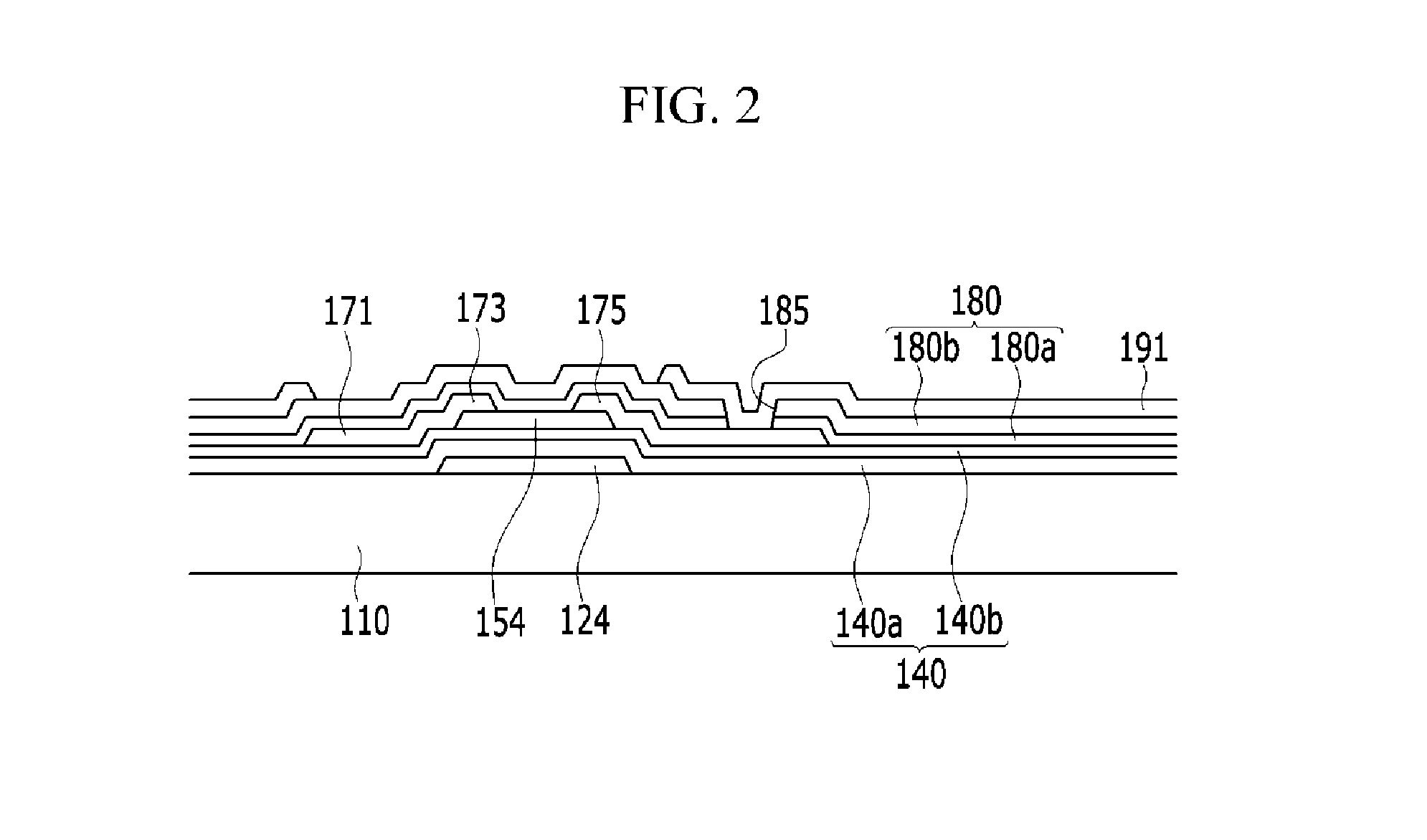
[0041]In the drawings, the thickness of layers, films, panels, regions, etc., are exaggerated for clarity. It will be understood that when a layer is referred to as being “on” another layer or substrate, it can be directly on the other layer or substrate, or intervening them may also be present. Like reference numerals designate like elements throughout the specification.

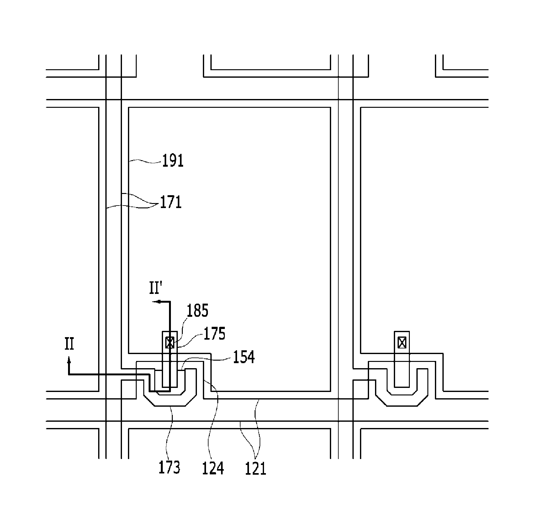
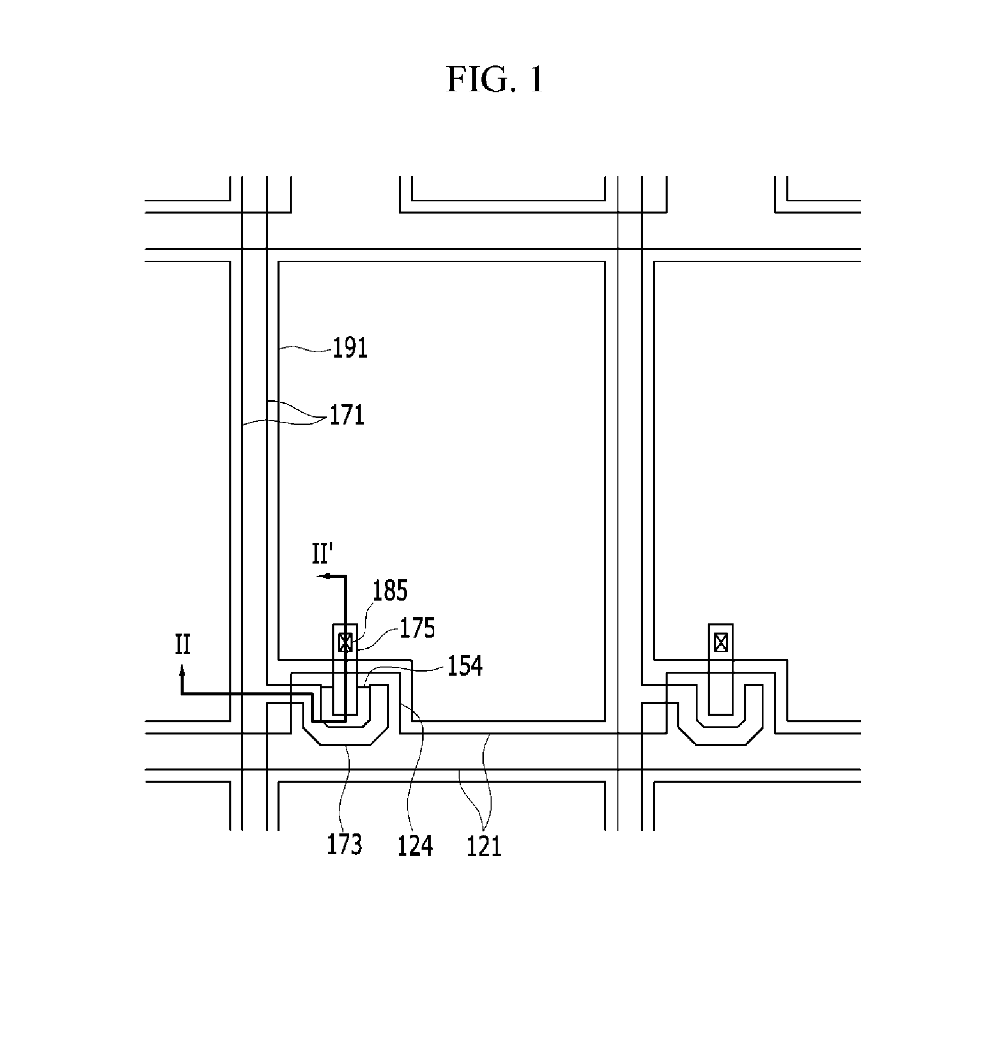
[0042]FIG. 1 is a layout view illustrating a thin film transistor display panel for a disp...


PUM


Abstract

A display device according to an exemplary embodiment of the present invention includes a semiconductor layer; a data line disposed on the semiconductor layer, and a source electrode as well as a drain electrode disposed on the semiconductor layer and facing the source electrode. The semiconductor layer is made of an oxide semiconductor including indium, tin, and zinc. An atomic percent of indium in the oxide semiconductor is equal to or larger than about 10 at % and equal to or smaller than about 90 at %, an atomic percent of zinc in the oxide semiconductor is equal to or larger than about 5 at % and equal to or smaller than about 60 at %, and an atomic percent of tin in the oxide semiconductor is equal to or larger than about 5 at % and equal to or smaller than about 45 at %, and the data line and the drain electrode comprise copper.

Description

CROSS-REFERENCE TO RELATED APPLICATION[0001]This application claims priority to, and the benefit of, Korean Patent Application No. 10-2012-0080796 filed in the Korean Intellectual Property Office on Jul. 24, 2012, the entire contents of which are incorporated herein by reference.BACKGROUND OF THE INVENTION[0002](a) Field of the Invention[0003]Embodiments of the present invention relate generally to flat panel displays. More specifically, embodiments of the present invention relate to a flat panel display device using an oxide semiconductor and a method of manufacturing the same.[0004](b) Description of the Related Art[0005]In general, a thin film transistor (TFT) is used as a switching element for independently driving each pixel in a flat panel display such as a liquid crystal display, an organic light emitting display or the like. A thin film display panel including such a thin film transistor typically includes a gate line for transferring a gate signal to the thin film transisto...

Claims


Application Information

Patent Timeline
Patent Type & Authority Patents(United States)
IPC IPC(8): H01L33/44H01L29/786H01L27/12
CPCH01L27/1225H01L29/7869H01L33/44H01L27/124H01L27/1248H01L29/06H01L29/45
Inventor AHN, BYUNG DULEE, KYOUNG WONKIM, GUN HEECHOI, YOUNG JOO
Owner SAMSUNG DISPLAY CO LTD
Why Eureka
Try Eureka