eFuse and method of fabrication
a technology of efuse and fabrication method, which is applied in the direction of semiconductor devices, semiconductor/solid-state device details, electrical apparatus, etc., can solve the problem of prior art efuse reliability to suffer
- Summary
- Abstract
- Description
- Claims
- Application Information
AI Technical Summary
Benefits of technology
Problems solved by technology
Method used
Image

Examples
Embodiment Construction
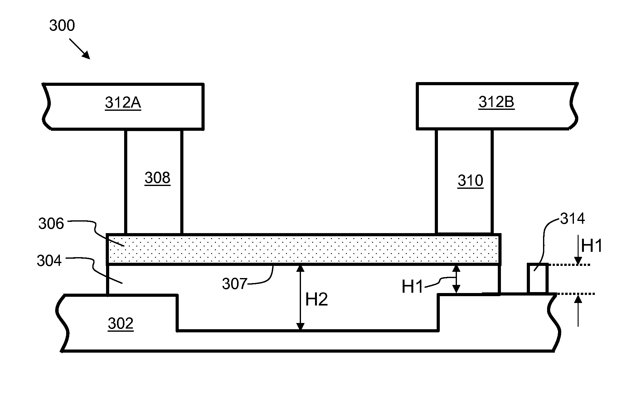
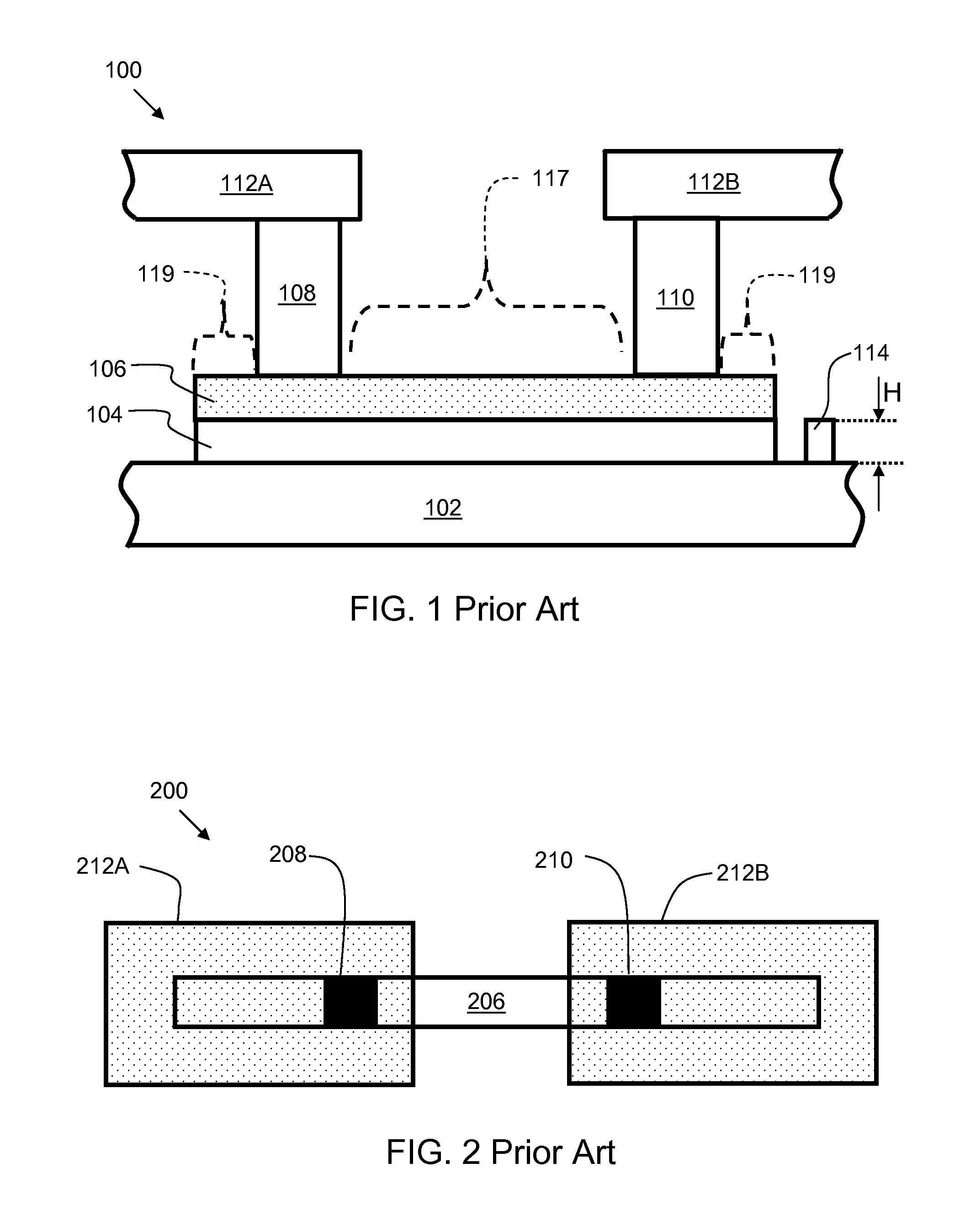
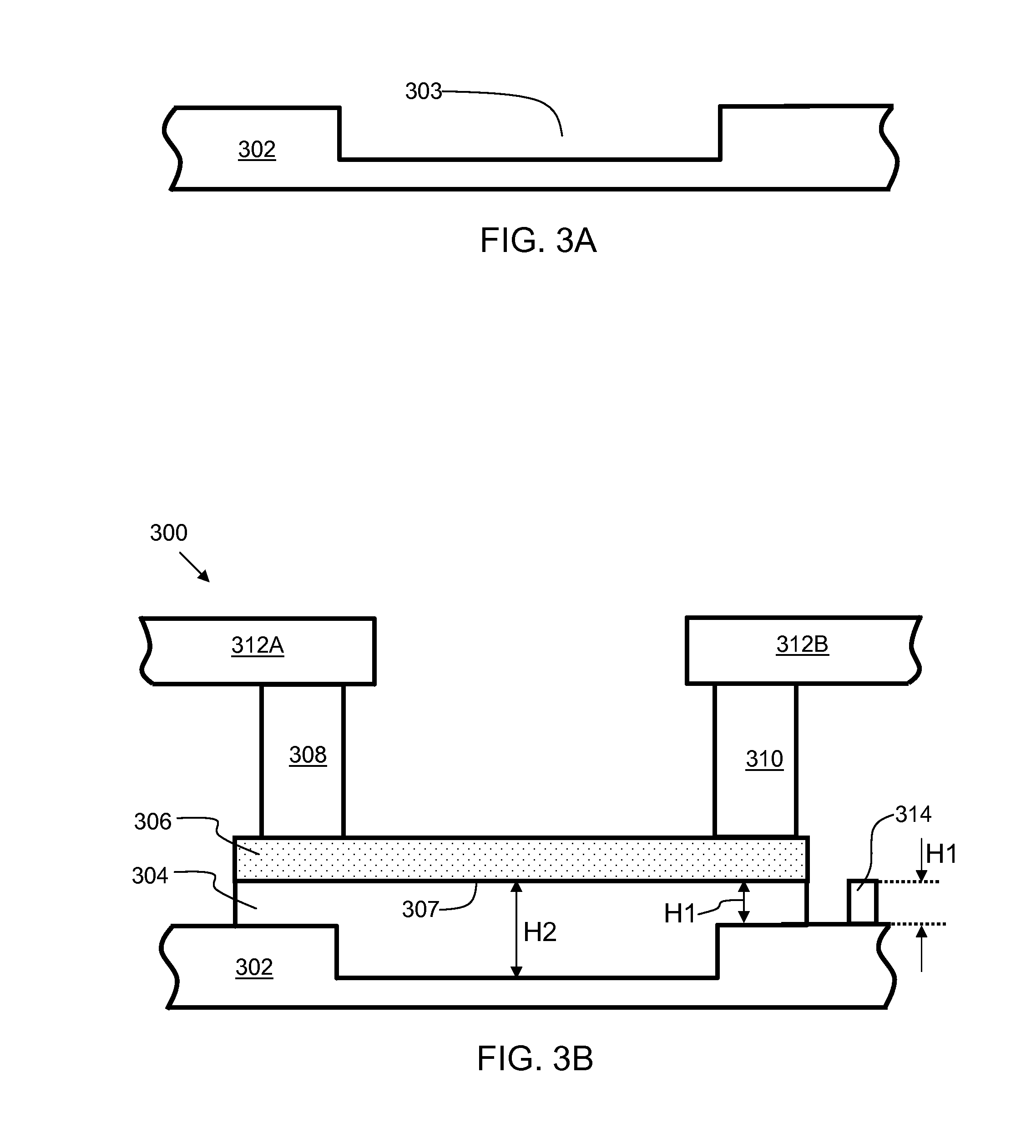
[0017]FIG. 1 is a side view of a prior art eFuse 100. eFuse 100 is formed on a dielectric layer 102. A polysilicon line 104 is formed on the dielectric layer. A silicide layer 106 is formed on the polysilicon line 104. Metal contacts 108 and 110 form the two contacts of the eFuse 100. Metal region 112A is electrically connected to contact 108, and metal region 112B is electrically connected to contact 110. Metal regions 112A and 112B are part of the same metal layer. When the eFuse is intact, an electrical connection exists between metal region 112A and metal region 112B. When the eFuse is in an open state (e.g. “blown”), there is an electrical open between metal region 112A and metal region 112B. Note that the term “blown” regarding the eFuse implies that an open is created, severing the electrical connection between contact 108 and contact 110. The eFuse is “blown” by applying a current which causes electromigration of the silicide to one side of the eFuse, creating the open circu...
PUM
 Abstract
Description
Claims
Application Information
 - R&D
- Intellectual Property
- Life Sciences
- Materials
- Tech Scout
- Unparalleled Data Quality
- Higher Quality Content
- 60% Fewer Hallucinations
Browse by: Latest US Patents, China's latest patents, Technical Efficacy Thesaurus, Application Domain, Technology Topic, Popular Technical Reports.
© 2025 PatSnap. All rights reserved.Legal|Privacy policy|Modern Slavery Act Transparency Statement|Sitemap|About US| Contact US: help@patsnap.com