Supercharge Your Innovation With Domain-Expert AI Agents!

Method of manufacturing device, and substrate

a manufacturing method and substrate technology, applied in the field of manufacturing devices and substrates, can solve the problems of disadvantageous throughput in terms of determining the position of the alignment mark in the y-direction with high precision, and measuring with a maximum precision in both the x- and y-directions

Inactive Publication Date: 2014-12-30
CANON KK
View PDF7 Cites 2 Cited by
  • Summary
  • Abstract
  • Description
  • Claims
  • Application Information

AI Technical Summary

Benefits of technology

This approach enables high-precision position measurement in both X- and Y-directions while optimizing throughput by adjusting the number of linear patterns based on required alignment precisions, reducing the impact of rotation errors and improving measurement reproducibility.

Problems solved by technology

This means that the alignment mark described in Japanese Patent Laid-Open No. 2003-92246 is disadvantageous in terms of determining the position of the alignment mark in the Y-direction with high precision.
If, for example, a maximum precision is required in one of the X- and Y-directions, while it is not required in the other, measurement with a maximum precision in both the X- and Y-directions is disadvantageous in terms of the throughput.

Method used


Image

  • Method of manufacturing device, and substrate
  • Method of manufacturing device, and substrate
  • Method of manufacturing device, and substrate

Examples


Embodiment Construction

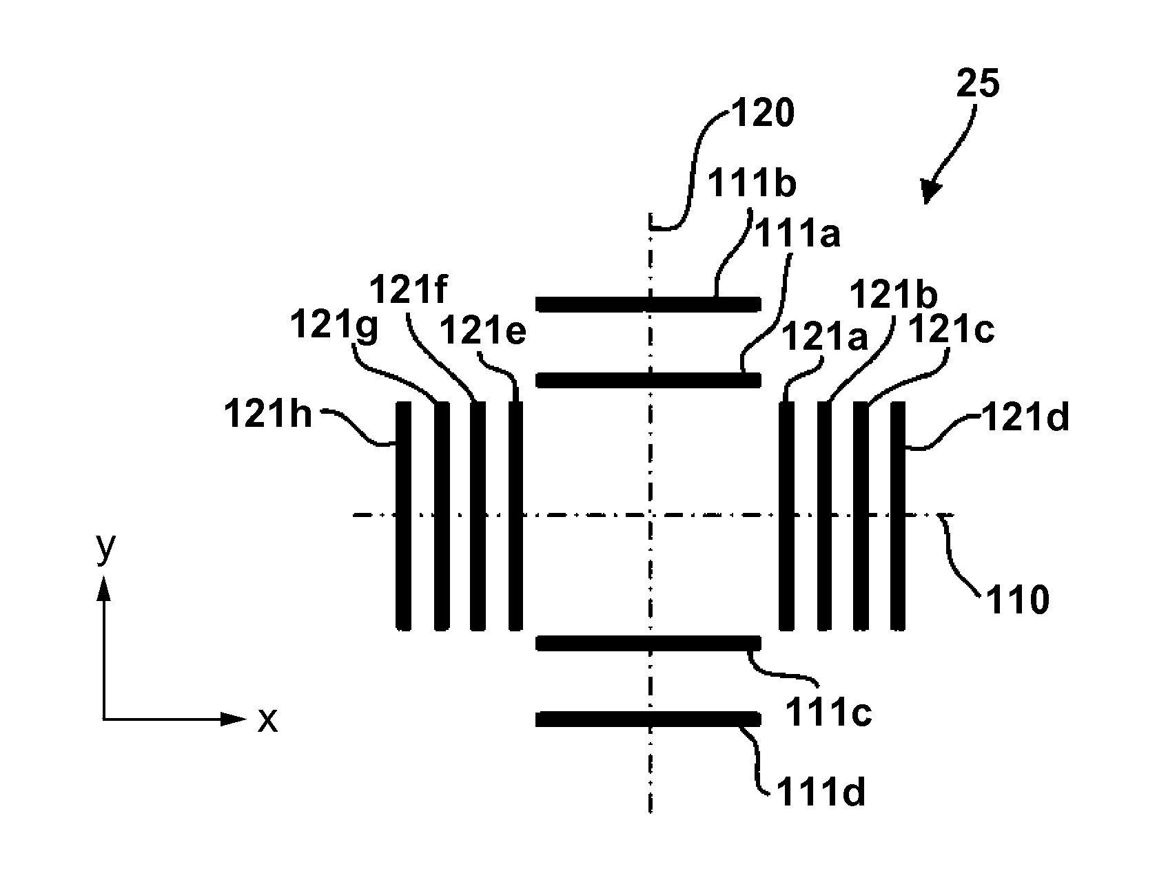
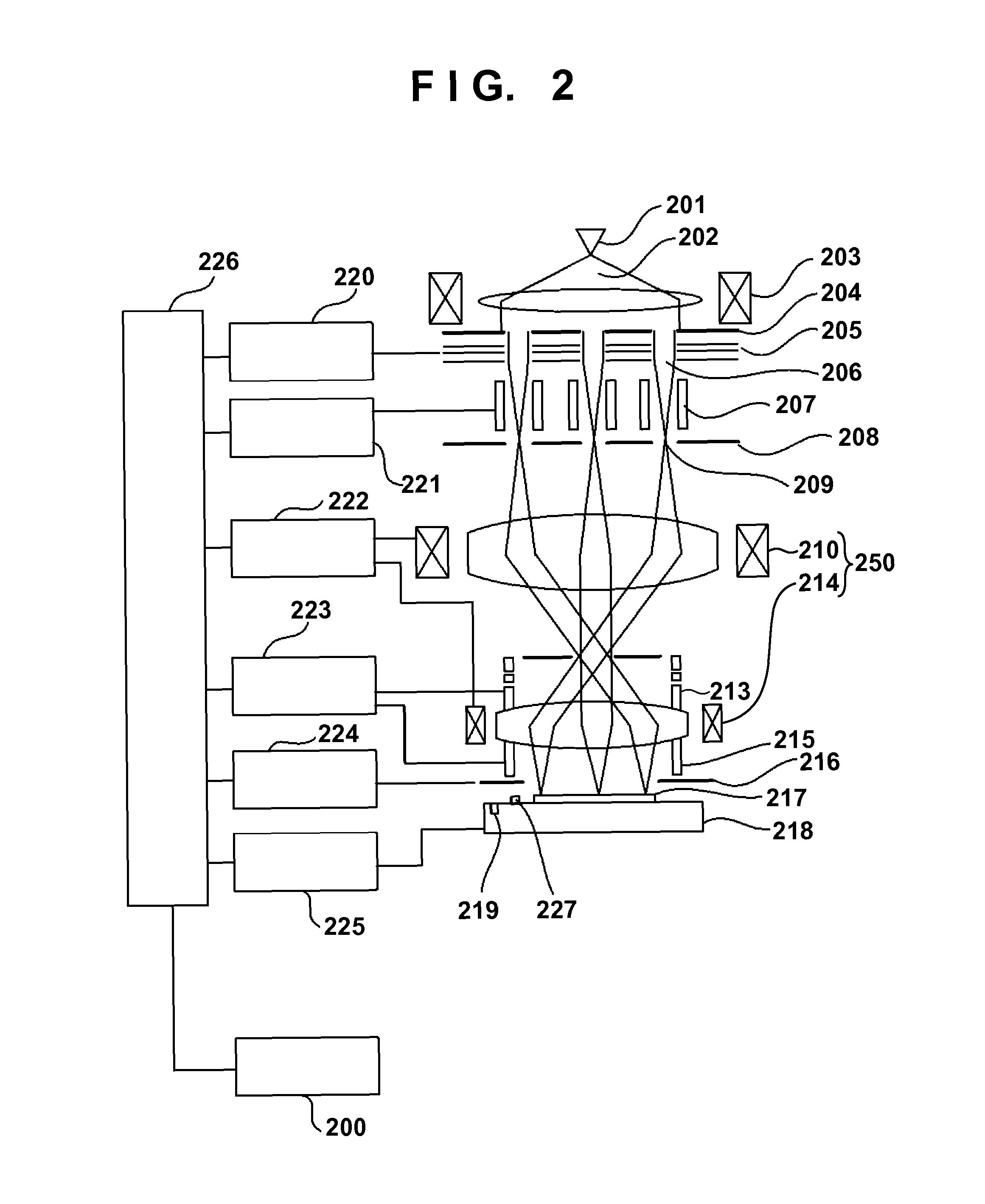
[0018]An embodiment of the present invention will be described below with reference to the accompanying drawings. This embodiment relates to a method of manufacturing a device. The method for manufacturing a device includes a first step of forming an alignment mark on a substrate such as a wafer, together with a circuit pattern, and a second step of measuring the position of the alignment mark, and forming a circuit pattern on the substrate while aligning the substrate based on the measured position.

[0019]The first step can include a step of determining the specifications of an alignment mark to be formed, and a lithography step of forming an alignment mark conforming to the determined specifications on a substrate. The lithography step can include, for example, a coating step, exposure step, development step, and etching step. In the coating step, a substrate is coated with a resist. In the exposure step, a latent image of a circuit pattern and alignment pattern is formed on the re...


PUM

PropertyMeasurementUnit
distanceaaaaaaaaaa
powersaaaaaaaaaa
voltageaaaaaaaaaa

Abstract

A method includes a first step of forming a circuit pattern and an alignment mark on a substrate and a second step of measuring a position of the alignment mark and positioning the substrate. The alignment mark includes a first linear pattern arranged on one side of a first straight line, a second linear pattern arranged on the other side of the first straight line, a third linear pattern arranged on one side of a second straight line, and a fourth linear pattern arranged on the other side of the second straight line. The first step includes determining total number of the third and fourth linear patterns to be formed and total number of the first and second linear patterns to be formed based on required precisions in directions along the first and second straight lines.

Description

BACKGROUND OF THE INVENTION[0001]1. Field of the Invention[0002]The present invention relates to a method of manufacturing a device, and a substrate.[0003]2. Description of the Related Art[0004]Japanese Patent Laid-Open No. 2003-92246 describes an alignment mark including first measurement marks X1, X2, X3, and X4 and second measurement marks Y1 and Y2. The first measurement marks X1, X2, X3, and X4 are used to measure the position of the alignment mark in the X-direction. The second measurement marks Y1 and Y2 are used to measure the position of the alignment mark in the Y-direction. The second measurement marks Y1 and Y2 are arranged outside the region in which the first measurement marks X1, X2, X3, and X4 are arranged, and parallel to the direction in which scribe lines are extended. The position of the alignment mark in the X-direction is the average of the positions of the first measurement marks X1, X2, X3, and X4. The position of the alignment mark in the Y-direction is the ...

Claims


Application Information

Patent Timeline
Patent Type & Authority Patents(United States)
IPC IPC(8): H01L23/544G03F7/20H01L21/76G03F9/00G01B11/00
CPCG03F9/7076G03F7/70633G03F9/7046
Inventor SENTOKU, KOICHIOGAWA, SHIGEKIINA, HIDEKI
Owner CANON KK
Features
  • R&D
  • Intellectual Property
  • Life Sciences
  • Materials
  • Tech Scout
  • Unparalleled Data Quality
  • Higher Quality Content
  • 60% Fewer Hallucinations
Learn More