

Doped semiconductor films and processing
a semiconductor film and film processing technology, applied in the field of semiconductor films, can solve the problems of short channel effects, increase in source and drain depth, and undesirable effects,
- Summary
- Abstract
- Description
- Claims
- Application Information
AI Technical Summary
Benefits of technology
Problems solved by technology
Method used
Image

Examples
Embodiment Construction
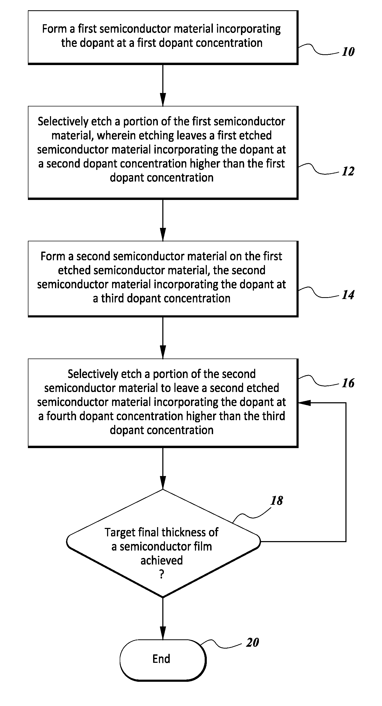
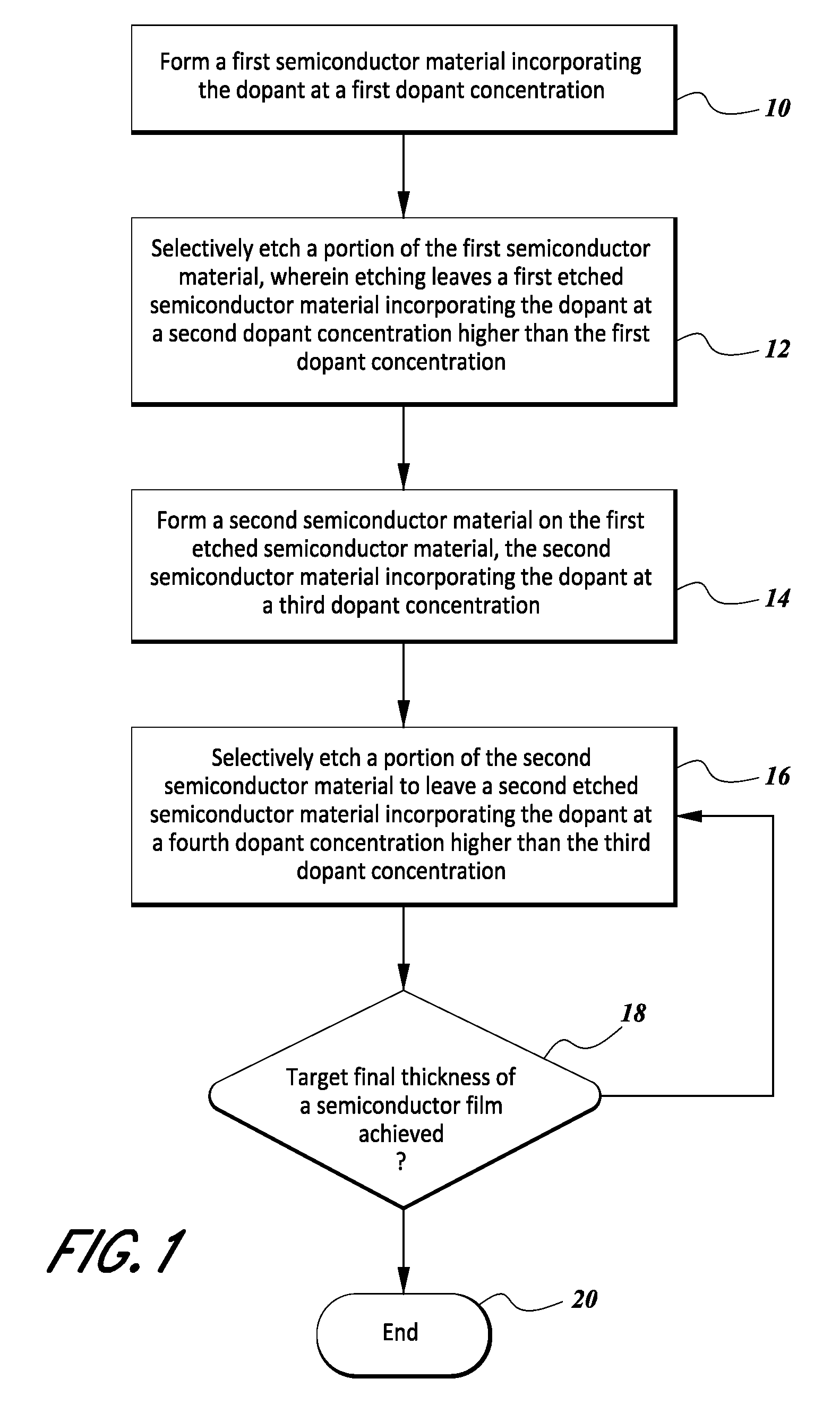
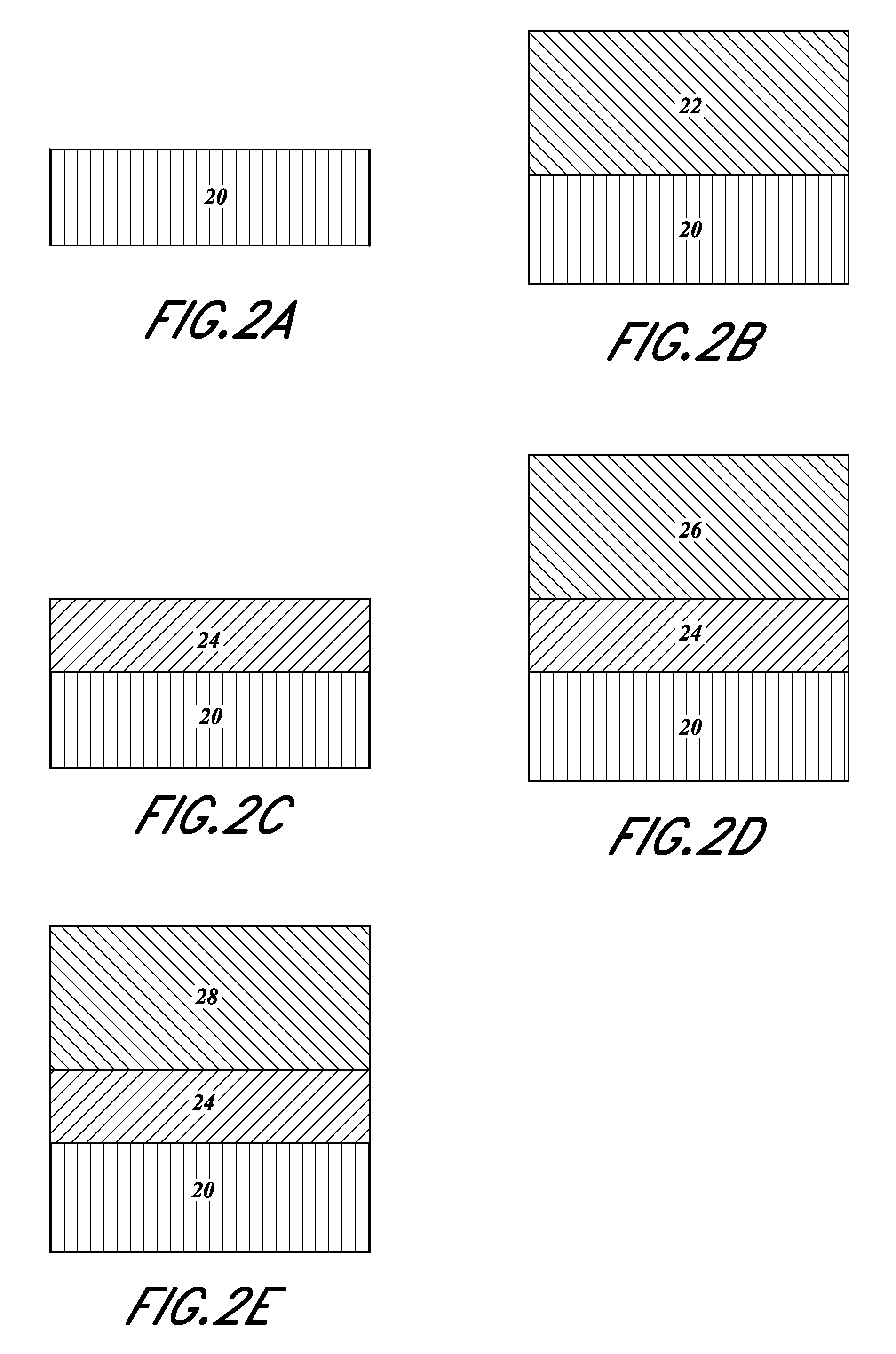
[0017]One approach to forming a doped semiconductor is to deposit a semiconductor material that is heavily doped in-situ. In situ doping can advantageously minimize dopant diffusion and facilitate sharp interfaces with adjacent materials, for example providing well-defined junctions for transistors. Moreover, in-situ doping techniques described herein are capable of incorporating dopant atoms into lattice sites of the semiconductor material, i.e., substitutionally, without having to perform a separate dopant activation step, such as a thermal anneal process, such that the dopant can be electrically active as-deposited.
[0018]FIG. 1 illustrates a method of incorporating an electrical dopant in a semiconductor film through cyclical deposition and etch (CDE) processes. According to one embodiment, the method includes forming 10 a first semiconductor material on a substrate. The first semiconductor material has a first thickness and incorporating the dopant at a first dopant concentratio...
PUM
| Property | Measurement | Unit |
|---|---|---|
| temperature | aaaaa | aaaaa |
| temperature | aaaaa | aaaaa |
| pressure | aaaaa | aaaaa |
Abstract
Description
Claims
Application Information