Methods of selective deposition of heavily doped epitaxial SiGe

Active Publication Date: 2005-04-14
APPLIED MATERIALS INC
View PDF55 Cites 312 Cited by
  • Summary
  • Abstract
  • Description
  • Claims
  • Application Information

AI Technical Summary

Benefits of technology

[0013] In another embodiment, the invention generally provides a method of selectively depositing a silicon-containing film on a substrate comprising placing the substrate within a process chamber, heating the substrate to a temperature in a range from about 500° C. to about 900° C. and maintaining a pressure in a range from about

Problems solved by technology

As smaller transistors are manufactured, ultra shallow source/drain junctions are becoming more challenging to produce.
Conventional doping by implantation and annealing is less effective as the junction depth approaches 10 nm.
On the other hand, the ultra shallow source/drain junction inevitably results in increased series resistance.
Also, junction consumption during silicide formation increases t

Method used


Image

  • Methods of selective deposition of heavily doped epitaxial SiGe
  • Methods of selective deposition of heavily doped epitaxial SiGe
  • Methods of selective deposition of heavily doped epitaxial SiGe

Examples


example 1

Boron Doped Silicon Germanium Deposition

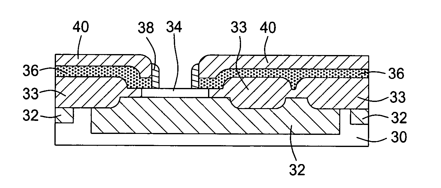
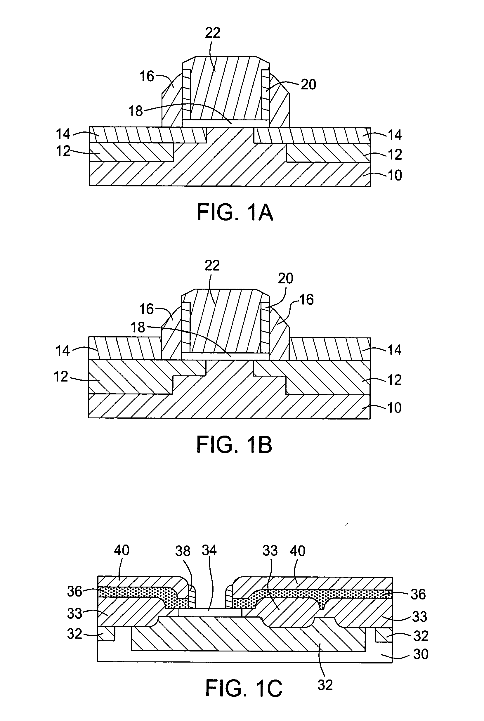
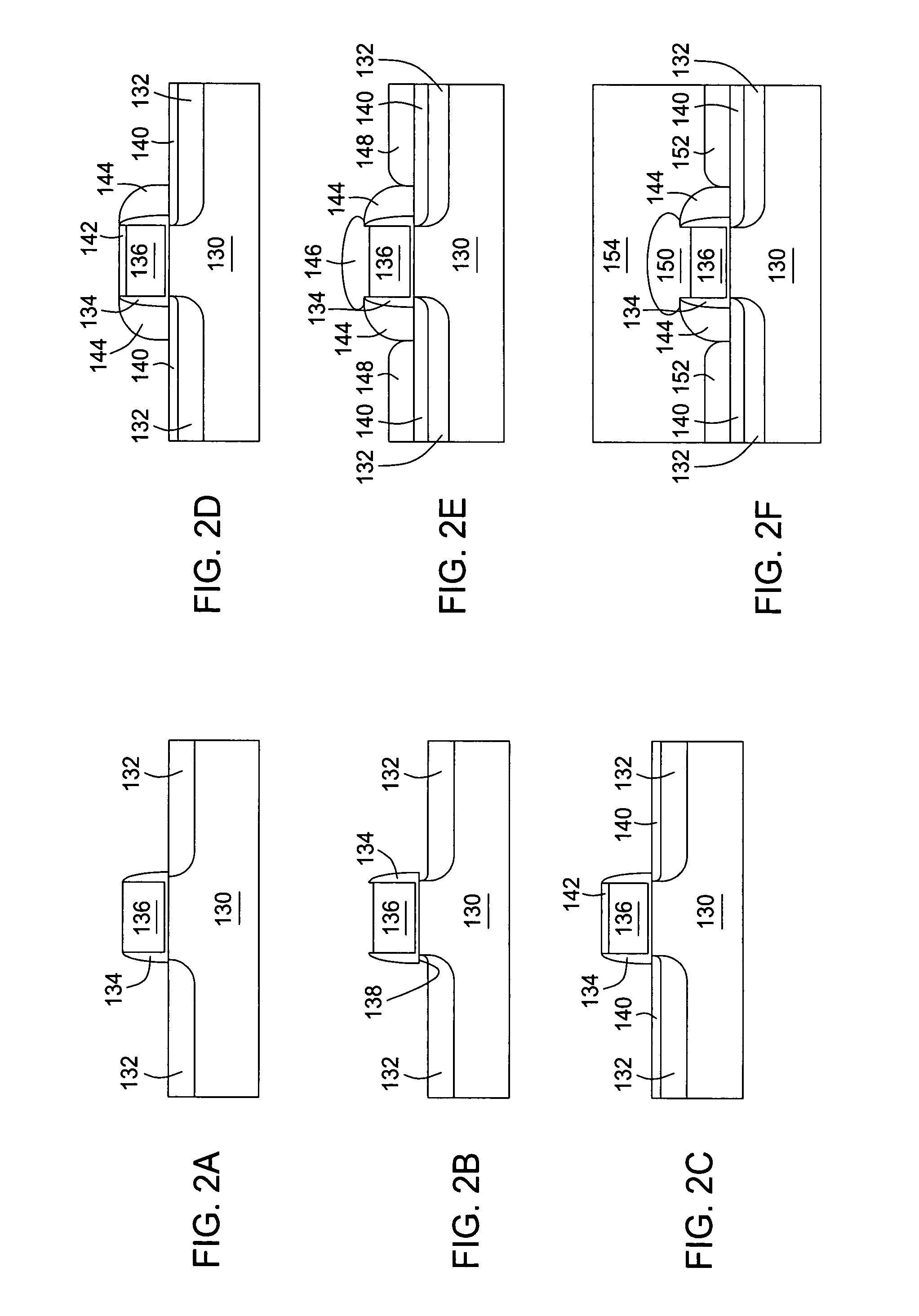
[0050] A substrate, Si, (e.g., 300 mm OD) was employed to investigate selective, monocrystalline film growth by CVD. A dielectric feature existed on the surface of the wafer. The wafer was prepared by subjecting to a 1% HF dip for 45 seconds. The wafer was loaded into the deposition chamber (Epi Centura® chamber) and baked in a hydrogen atmosphere at 800° C. for 60 seconds to remove native oxide. A flow of carrier gas, hydrogen, was directed towards the substrate and the source compounds were added to the carrier flow. Silane (100 sccm) and germane (6 sccm) were added to the chamber at 15 Torr and 725° C. Hydrogen chloride was delivered with a flow rate of 460 sccm. Diborane was delivered with a flow rate of 1 sccm. The substrate was maintained at 725° C. Deposition was carried out for 5 minutes to form a 500 Å SiGe film with a germanium concentration of 21 atomic percent and the boron concentration was 2.0×1020 cm−3.

example 2

Phosphorus Doped Silicon Germanium Deposition

[0051] A substrate was prepared as in Example 1. The wafer was loaded into the deposition chamber (Epi Centura® chamber) and baked in a hydrogen atmosphere at 800° C. for 60 seconds to remove native oxide. A flow of carrier gas, hydrogen, was directed towards the substrate and the source compounds were added to the carrier flow. Silane (100 sccm) and germane (4 sccm) were added to the chamber at 15 Torr and 725° C. Hydrogen chloride was delivered with a flow rate of 250 sccm. Phosphine was delivered to the chamber with a flow rate of 1 sccm. The substrate was maintained at 725° C. Deposition was carried out for 5 minutes to form a 500 Å SiGe film with a germanium concentration of 20 atomic percent and the phosphorus concentration was 1.6×1020 cm−3.

example 3

Boron Doped Silicon Germanium Deposition with Sequential Cl2SiH2 and SiH4 Flows

[0052] The substrates were prepared as in Example 1. The wafer was loaded into the deposition chamber (Epi Centura® chamber) and baked in a hydrogen atmosphere at 800° C. for 60 seconds to remove native oxide. A flow of carrier gas, hydrogen, was directed towards the substrate and the source compounds were added to the carrier flow. Dichlorosilane (100 sccm), germane (2.8 sccm), and diborane (0.3 sccm) were added to the chamber at 15 Torr and 725° C. Hydrogen chloride was delivered with a flow rate of 190 sccm. The substrate was maintained at 725° C. Deposition was conducted for 72 seconds to form a first layer of silicon compound with a thickness of 50 Å. On top of the first layer, a subsequent epitaxial layer (i.e., a second layer of silicon compound) was deposited using silane (100 sccm), germane (6 sccm), hydrogen chloride (460 sccm) and diborane (1 sccm). The chamber pressure and temperature remaine...


PUM


Abstract

The invention generally teaches a method for depositing a silicon film or silicon germanium film on a substrate comprising placing the substrate within a process chamber and heating the substrate surface to a temperature in the range from about 600° C. to about 900° C. while maintaining a pressure in the range from about 0.1 Torr to about 200 Torr. A deposition gas is provided to the process chamber and includes SiH4, an optional germanium source gas, an etchant, a carrier gas and optionally at least one dopant gas. The silicon film or the silicon germanium film is selectively and epitaxially grown on the substrate. One embodiment teaches a method for depositing a silicon-containing film with an inert gas as the carrier gas. Methods may include the fabrication of electronic devices utilizing selective silicon germanium epitaxial films.

Description

BACKGROUND OF THE INVENTION [0001] 1. Field of the Invention [0002] Embodiments of the invention generally relate to the field of semiconductor manufacturing processes and devices, more particular, to methods of depositing silicon-containing films forming semiconductor devices. [0003] 2. Description of the Related Art [0004] As smaller transistors are manufactured, ultra shallow source / drain junctions are becoming more challenging to produce. According to the International Technology Roadmap for Semiconductors (ITRS), junction depth is required to be less than 30 nm for sub-100 nm CMOS (complementary metal-oxide semiconductor) devices. Conventional doping by implantation and annealing is less effective as the junction depth approaches 10 nm. Doping by implantation requires a post-annealing process in order to activate dopants and post-annealing causes enhanced dopant diffusion into layers. [0005] Recently, heavily-doped (about >1019 atoms / cm3), selective SiGe epitaxy has become a...

Claims


Application Information

Patent Timeline
IPC IPC(8): H01L21/20H01L21/205
CPCH01L21/0237H01L21/02532H01L21/02576H01L29/7848H01L21/0262H01L21/02636H01L29/78H01L21/02579H01L21/20
Inventor KIM, YIHWANSAMOILOV, ARKADII V.
Owner APPLIED MATERIALS INC
Why Eureka
Try Eureka