IMPROVED CMOS (Complementary Metal Oxide Semiconductor) TECHNOLOGY

a technology of metal oxide semiconductor and cmos, which is applied in the direction of semiconductor devices, basic electric elements, electrical equipment, etc., can solve problems such as device performance degradation

Inactive Publication Date: 2007-01-25
IBM CORP
View PDF13 Cites 309 Cited by
  • Summary
  • Abstract
  • Description
  • Claims
  • Application Information

AI Technical Summary

Benefits of technology

[0009] The present invention provides methods of forming transistors in which leakage current problem is mitigated.

Problems solved by technology

As device dimensions continue to shrink (i.e., scaling), the gate dielectric region that electrically insulates the channel region and the polysilicon gate region of the transistor becomes thinner and therefore experiences increasing leakage current due to direct carrier tunneling, resulting in degraded device performance.

Method used


Image

  • IMPROVED CMOS (Complementary Metal Oxide Semiconductor) TECHNOLOGY
  • IMPROVED CMOS (Complementary Metal Oxide Semiconductor) TECHNOLOGY
  • IMPROVED CMOS (Complementary Metal Oxide Semiconductor) TECHNOLOGY

Examples


Embodiment Construction

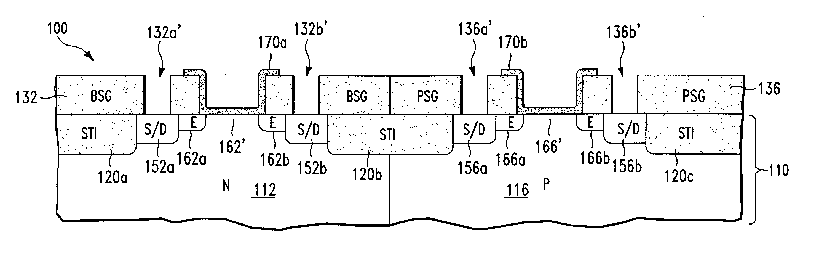
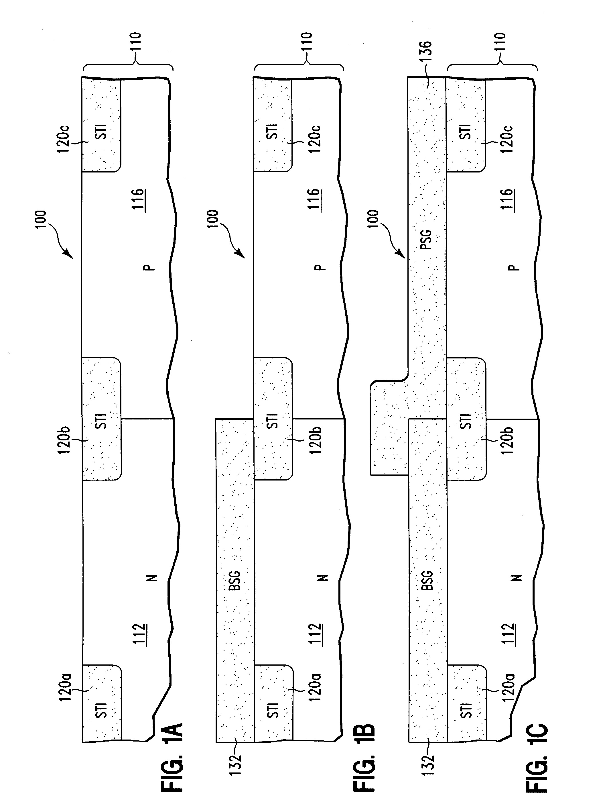
[0013]FIGS. 1A-1J illustrate the steps of a first transistor fabrication method for forming a semiconductor structure 100, in accordance with embodiments of the present invention. More specifically, with reference to FIG. 1A, in one embodiment, the first transistor fabrication method starts out with a semiconductor (e.g., silicon, germanium, etc.) layer 110.

[0014] Next, in one embodiment, shallow trench isolation (STI) regions 120a, 120b, and 120c are formed in the Si layer 110, using any conventional method.

[0015] Next, in one embodiment, a region 112 of the Si layer 110 is doped with N type dopants (e.g., phosphorous atoms) so as to form the N well 112 in the Si layer 110, using any conventional method. Next, in one embodiment, a region 116 of the Si layer 110 is doped with P type dopants (e.g., boron atoms) so as to form the P well 116 in the Si layer 110, using any conventional method.

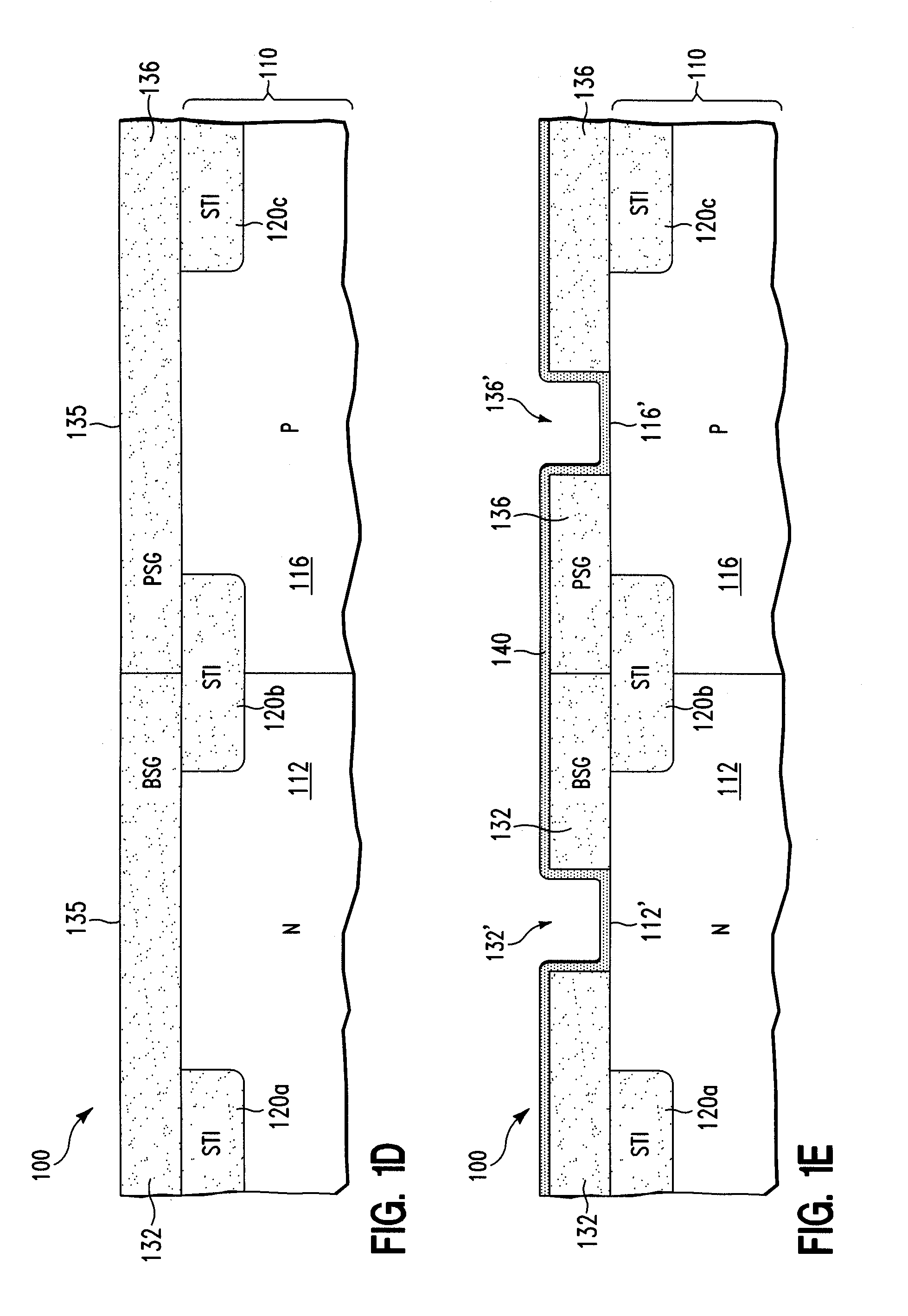
[0016] Next, with reference to FIG. 1B, in one embodiment, a BSG (boron silicate glass) regi...


PUM


Abstract

A method for forming semiconductor transistor. The method comprises providing a structure including (a) a semiconductor region, and (b) first and second dopant source regions on and in direct physical contact with the semiconductor region, wherein each region of the first and second dopant source regions comprises a dielectric material which contains dopants; causing the dopants to diffuse from the first and second dopant source regions into the semiconductor region so as to form first and second source/drain extension regions, respectively, wherein the first and second source/drain extension regions define a channel region disposed between; forming a gate dielectric region on a channel region; and forming a gate region on the gate dielectric region, wherein the gate dielectric region electrically insulates the gate region from the channel region.

Description

BACKGROUND OF THE INVENTION [0001] 1. Technical Field [0002] The present invention relates to CMOS (Complementary Metal Oxide Semiconductor) technology, and more specifically, to improvements to CMOS technology. [0003] 2. Related Art [0004] In traditional CMOS (Complementary Metal Oxide Semiconductor) technology, the fabrication of a semiconductor transistor comprises (a) forming a gate stack (including a polysilicon gate region on a gate dielectric region) on a semiconductor layer, and (b) forming first and second source / drain (S / D) regions (i) in the semiconductor layer and (ii) aligned with the gate stack. The first and second S / D regions define a channel region in the semiconductor layer and directly beneath the gate dielectric region. As device dimensions continue to shrink (i.e., scaling), the gate dielectric region that electrically insulates the channel region and the polysilicon gate region of the transistor becomes thinner and therefore experiences increasing leakage curre...

Claims


Application Information

Patent Timeline
Patent Type & Authority Applications(United States)
IPC IPC(8): H01L21/8234
CPCH01L21/28079H01L21/28194H01L21/823814H01L29/66583H01L29/495H01L29/517H01L29/66553H01L21/823828
Inventor SPERANZA, ANTHONY C.
Owner IBM CORP
Why Eureka
Try Eureka