Semiconductor device and method for fabricating the same

a technology of semiconductor devices and semiconductors, applied in the direction of semiconductor devices, electrical equipment, transistors, etc., can solve problems such as unfavorable electrical leakage, and achieve the effect of improving the quality of semiconductor devices

Inactive Publication Date: 2001-11-29
LAPIS SEMICON CO LTD
View PDF0 Cites 6 Cited by
  • Summary
  • Abstract
  • Description
  • Claims
  • Application Information

AI Technical Summary

Benefits of technology

0007] Accordingly, an object of the present invention is to improve qual...

Problems solved by technology

As a result, undesirabl...

Method used


Image

  • Semiconductor device and method for fabricating the same
  • Semiconductor device and method for fabricating the same
  • Semiconductor device and method for fabricating the same

Examples


Embodiment Construction

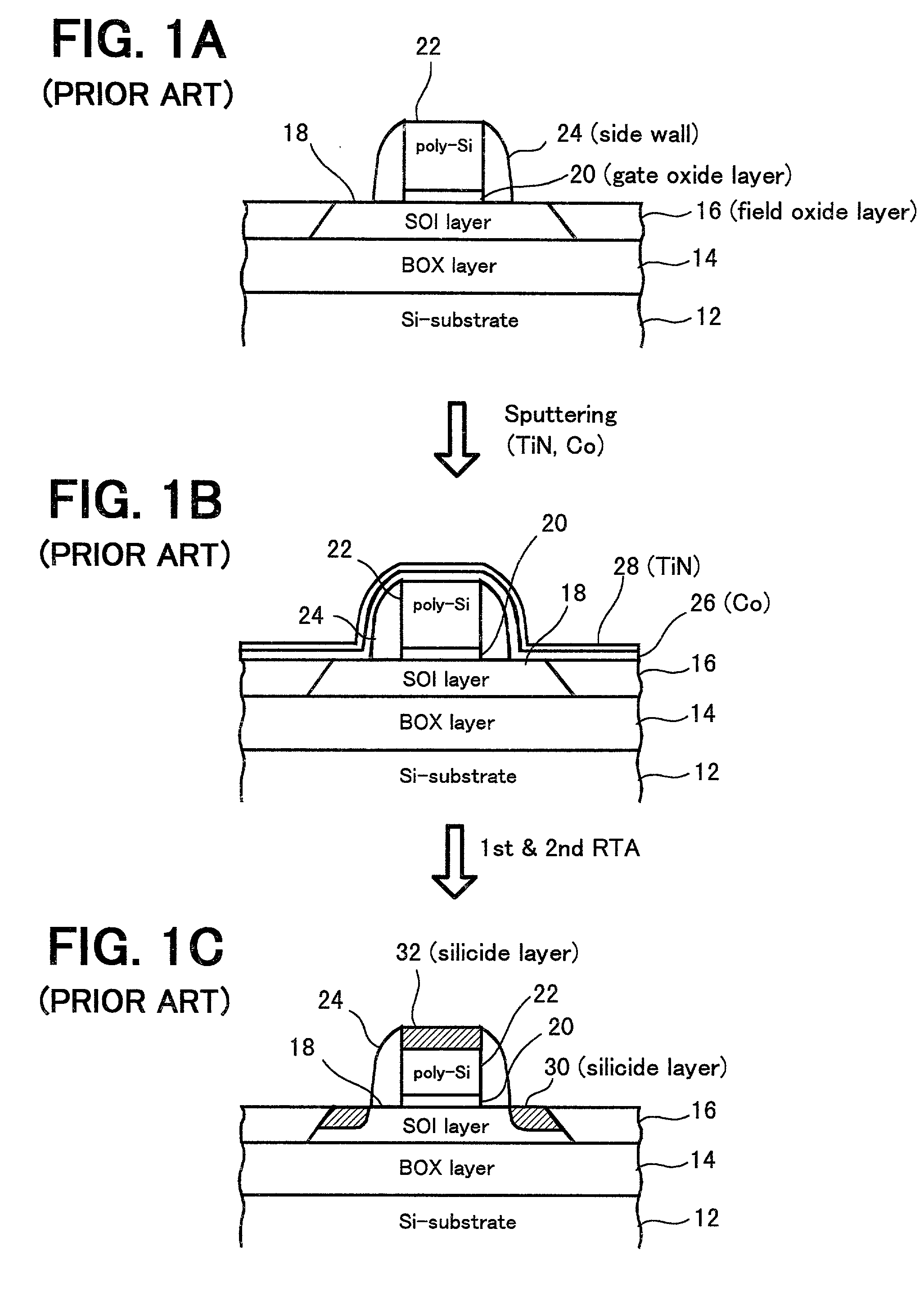
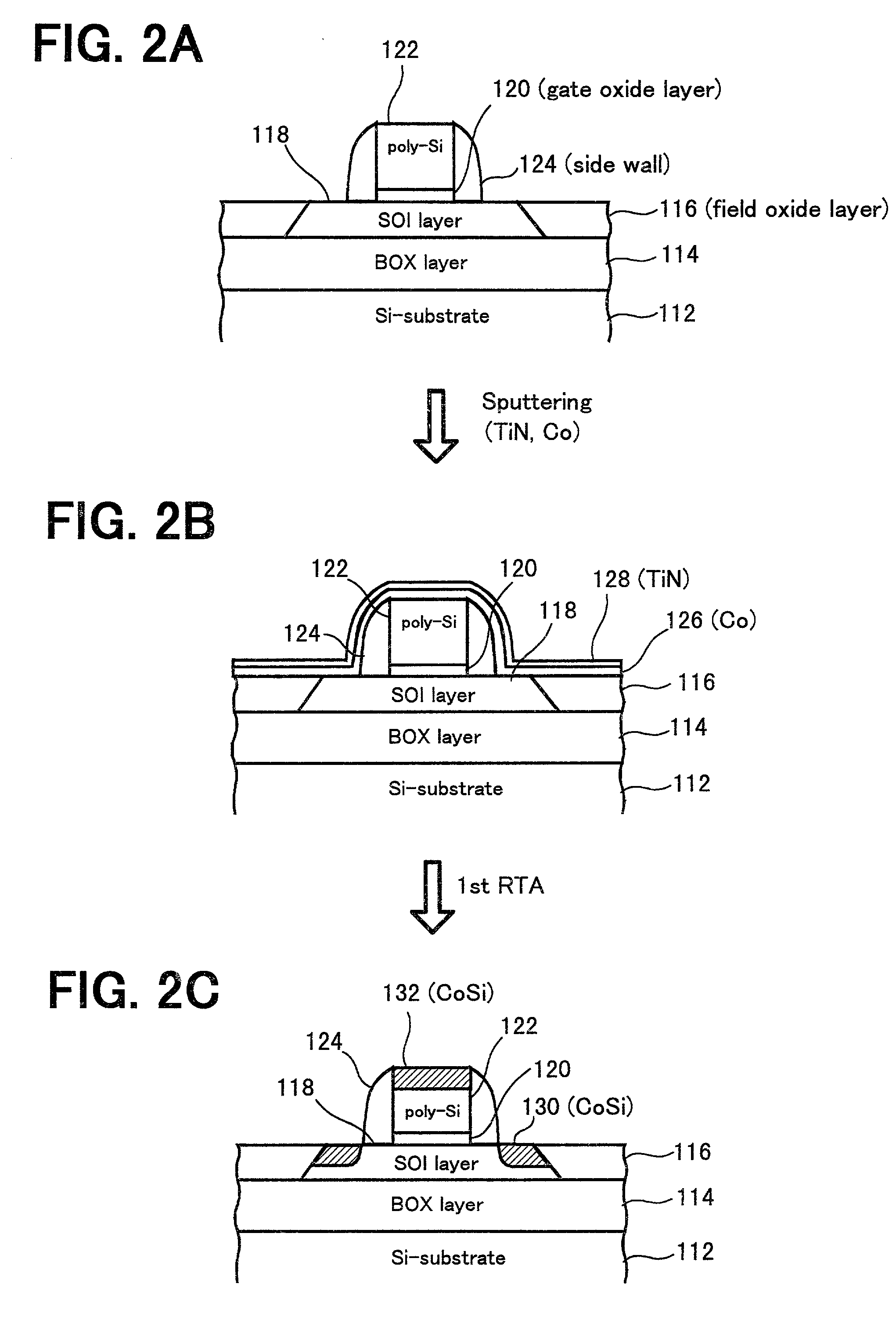
[0021] For better understanding of the present invention, a conventional technology is first described. FIGS. 1A to 1C are cross-sectional views showing fabrication steps of a conventional semiconductor device. FIGS. 1A to 1C show salicide process of a SOI (Silicon on Insulator) type of semiconductor device.

[0022] FIG. 1A shows a condition in which gate-side-wall process is completed. As shown in FIG. 1A, a BOX (Buried Oxide) layer 14 is formed on a silicon substrate 12 to have a thickness of 100 nm to 200 nm. A filed oxide layer 16 and a SOI (Silicon on Insulator) layer 18 are formed on the BOX layer 14. The SOI layer 18 is of FD (Fully Depletion) type and is designed to have a thickness of 50 nm to 100 nm. A gate oxide layer 20 is formed on the SOI layer 18 to have a thickness of 3.5 nm to 7.0 nm. A poly-silicon gate layer 22 is formed on the gate oxide layer 20 to have a thickness of 150 nm to 250 nm. A gate side wall layer 24 is formed on the SOI layer 18 to surround the poly-si...


PUM


Abstract

In a method for fabricating a semiconductor device, a silicide material is formed at least on the surface of an area to be silicided. Then, a first RTA (Rapid Thermal Annealing) process is performed to form a first-reacted silicide region. Next, a supplemental silicon layer is formed over the entire surface; and a second RTA process is performed to form a second-reacted silicide region.

Description

[0001] The present invention relates to semiconductor fabrication technology, and more particularly to a semiconductor device that is fabricated using SALICIDE (Self Aligned Silicide) process.[0002] In recent years, semiconductor devices have been miniaturized and improved in performance, and at the same time, system LSIs have been proposed. In such a system LSI, for improving its performance, it is required to decrease resistance of a gate pattern and active regions of source and drain. As shown in "Semiconductor World", May 1998, page 66, salicide process has been used to decrease that resistance. Especially for SOI (Silicon-On-Insulator) type of devices, the salicide process is important. SOI technology has become increasingly important in the field of integrated circuits. In SOI fabrication, a layer of semiconductor material overlies an insulating layer, typically, a single crystal layer of silicon overlies a layer of silicon dioxide, which itself overlies a silicon substrate.[0...

Claims


Application Information

Patent Timeline
IPC IPC(8): H01L21/28H01L21/285H01L21/324H01L21/336H01L21/84H01L27/12H01L29/45H01L29/49H01L29/786
CPCH01L21/28052H01L21/28518H01L21/324H01L21/84H01L27/1203H01L29/458H01L29/4908H01L29/4933H01L29/665H01L29/66772H01L29/78609H01L21/18
Inventor KANAMORI, JUN
Owner LAPIS SEMICON CO LTD
Why Eureka
Try Eureka