Materials and devices for blue phosphorescence based organic light emitting diodes

a blue phosphorescence and organic light-emitting diode technology, applied in the direction of organic semiconductor devices, thermoelectric devices, luminescent compositions, etc., can solve the problems of energy loss, energy loss, and inability to convert excitons in fluorescent devices to energetically unfavorable higher singlet excited states,

Inactive Publication Date: 2007-11-13
UNIV OF SOUTHERN CALIFORNIA +1
View PDF19 Cites 305 Cited by
  • Summary
  • Abstract
  • Description
  • Claims
  • Application Information

AI Technical Summary

Benefits of technology

[0010]The present invention relates to OLED devices that efficiently emit light, in particular that preferably emit light in the blue range of the visible spectrum, and to a method for forming such devices. The OLEDs made according to the invention preferably include blue phosphorescent OLEDs with efficiency levels comparable to those of current green to red phosphorescent OLEDs.

Problems solved by technology

The remaining excitons in a fluorescent device, which are produced in the lowest triplet excited state of an organic molecule, are typically not capable of being converted into the energetically unfavorable higher singlet excited states from which the fluorescence is produced.
This energy, thus, becomes lost to radiationless decay processes that only tend to heat-up the device.
If a dopant capable of producing blue phosphorescence is inserted in such a device utilizing the existing materials and structures, the emission will only come, if at all, inefficiently from the matrix material, and not from the phosphorescent dopant material.

Method used


Image

  • Materials and devices for blue phosphorescence based organic light emitting diodes
  • Materials and devices for blue phosphorescence based organic light emitting diodes
  • Materials and devices for blue phosphorescence based organic light emitting diodes

Examples


Embodiment Construction

[0023]Embodiments of the present invention will be described with reference to the drawings. It is understood that these embodiments are intended as illustrative examples of the invention, and do not limit the invention.

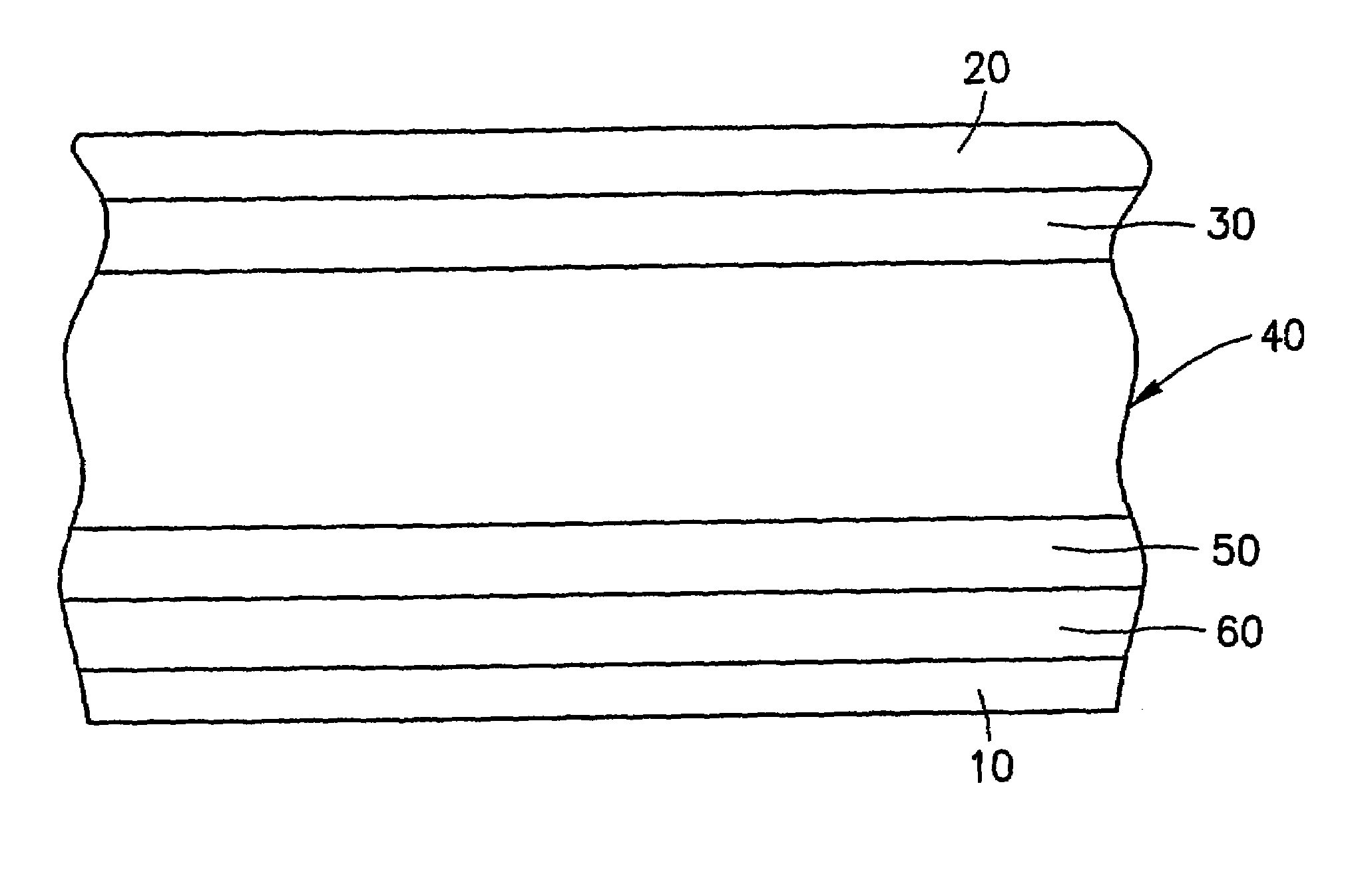
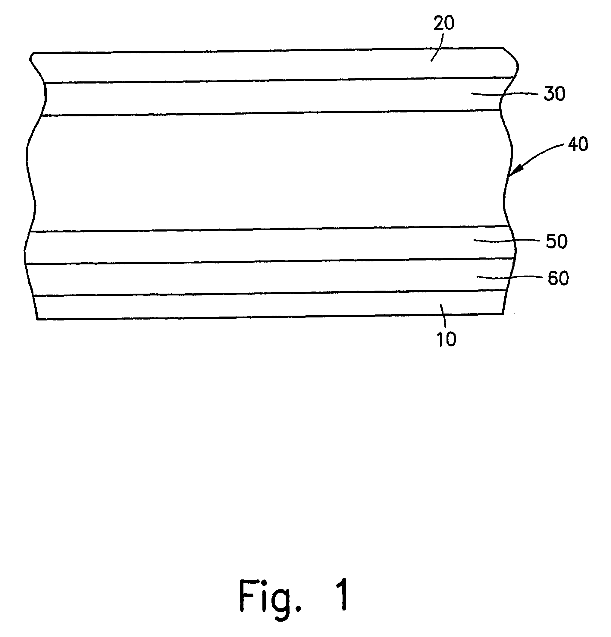
[0024]The OLEDs made according to the present invention include phosphorescent dopants dispersed in the device's emissive layer, preferably capable of achieving internal quantum efficiencies approaching 100%. The emissive dopants in these devices typically contain heavy transition metal atoms, such as, for example, iridium or platinum, that induce efficient radiative relaxation of triplet excitons. Although iridium and platinum have provided high quantum efficiencies, other heavy metals such as osmium or gold may also be used. These phosphorescent dopants thus can take advantage of substantially all the excitons available within the emissive layer of the device, resulting in much higher efficiencies compared to devices using only singlet excitation to induce luminesc...


PUM

PropertyMeasurementUnit
energy gapaaaaaaaaaa
emission peakaaaaaaaaaa

Abstract

An OLED includes a wide gap inert host material doped with two dopants. One of the dopants is an emissive phosphorescent material that can transport either electrons or holes. The other dopant is a charge carrying material that can transport whichever of the electrons and holes that is not transported by the phosphorescent dopant. The materials are selected so that the lowest triplet energy level of the host material and the lowest triplet energy level of the charge carrying dopant material are each at a higher energy level than the lowest triplet state energy level of the phosphorescent dopant material. The device is capable, in particular, of efficiently emitting light in the blue region of the visible spectrum.

Description

REFERENCE TO RELATED APPLICATION[0001]This application claims the benefit of U.S. Provisional Application No. 60 / 275,481 filed on Mar. 14, 2001.RESEARCH AGREEMENTS[0002]The claimed invention was made by, on behalf of, and / or in connection with one or more of the following parties to a joint university-corporation research agreement: Princeton University, The University of Southern California, and Universal Display Corporation. The agreement was in effect on and before the date the claimed invention was made, and the claimed invention was made as a result of activities undertaken within the scope of the agreement.GOVERNMENT RIGHTS[0003]This invention was made with Government support under Contract No. F33615-94-1-1414 awarded by DARPA and Contract No. DMR94-00362 awarded by the National Science Foundation. The government has certain rights in this invention.FIELD OF THE INVENTION[0004]The present invention relates to highly efficient organic light emitting devices (OLEDs) that are, f...

Claims


Application Information

Patent Timeline
Patent Type & Authority Patents(United States)
IPC IPC(8): H01L35/24C09K11/06H01L51/00H01L51/30H01L51/40H01L51/50
CPCH01L51/0087H01L51/5016H01L51/0085H01L51/002H01L51/005H01L51/007H01L2251/552H10K71/30H10K85/60H10K85/6565H10K85/346H10K85/342H10K50/11H10K2101/10H10K2101/30H05B33/18
Inventor THOMPSON, MARK E.FORREST, STEPHEN
Owner UNIV OF SOUTHERN CALIFORNIA
Why Eureka
Try Eureka