Illumination device with semiconductor light-emitting elements

a technology of light-emitting elements and illumination devices, which is applied in the direction of lighting and heating apparatus, lighting support devices, printed circuit aspects, etc., can solve the problems of insufficient use of light-emitting diodes, insufficient light-emitting diodes, and insufficient brightness, so as to suppress the temperature rise of semiconductor light-emitting elements and efficiently extract light

Inactive Publication Date: 2010-04-06
TOSHIBA LIGHTING & TECH CORP
View PDF8 Cites 110 Cited by
  • Summary
  • Abstract
  • Description
  • Claims
  • Application Information

AI Technical Summary

Benefits of technology

[0012]The object of the present invention is to provide an illumination device which can efficiently extract light while suppressing a temperature rise of semiconductor light-emitting elements.

Problems solved by technology

However, in the conventional illumination device, although the temperature rise of the light-emitting diode chip can be suppressed, the extraction of light emitted from the light-emitting diode chips is not adequate.
Hence, the use of the light from the light-emitting diode chips is not sufficient, and the brightness may become deficient, for example, when purposes of use for general illumination are assumed.

Method used


Image

  • Illumination device with semiconductor light-emitting elements
  • Illumination device with semiconductor light-emitting elements
  • Illumination device with semiconductor light-emitting elements

Examples


first embodiment

[0078]the present invention will now be described with reference to FIG. 1 to FIG. 5.

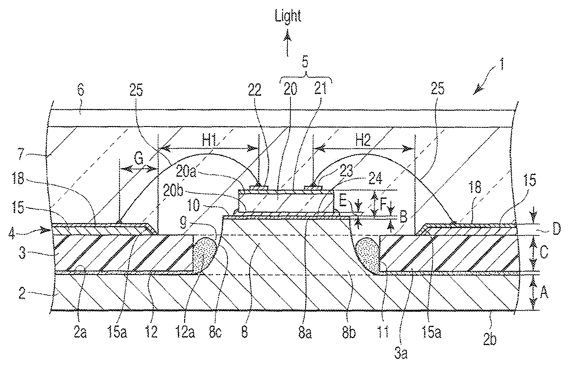
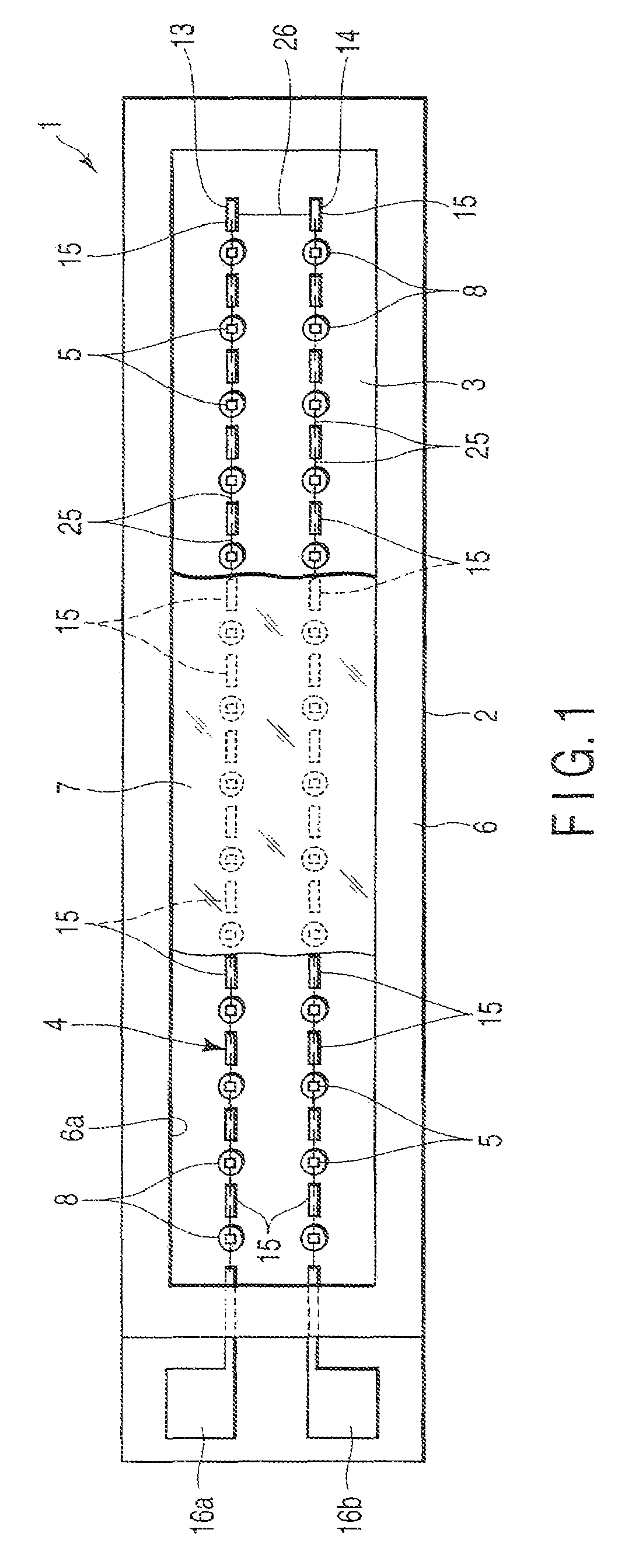
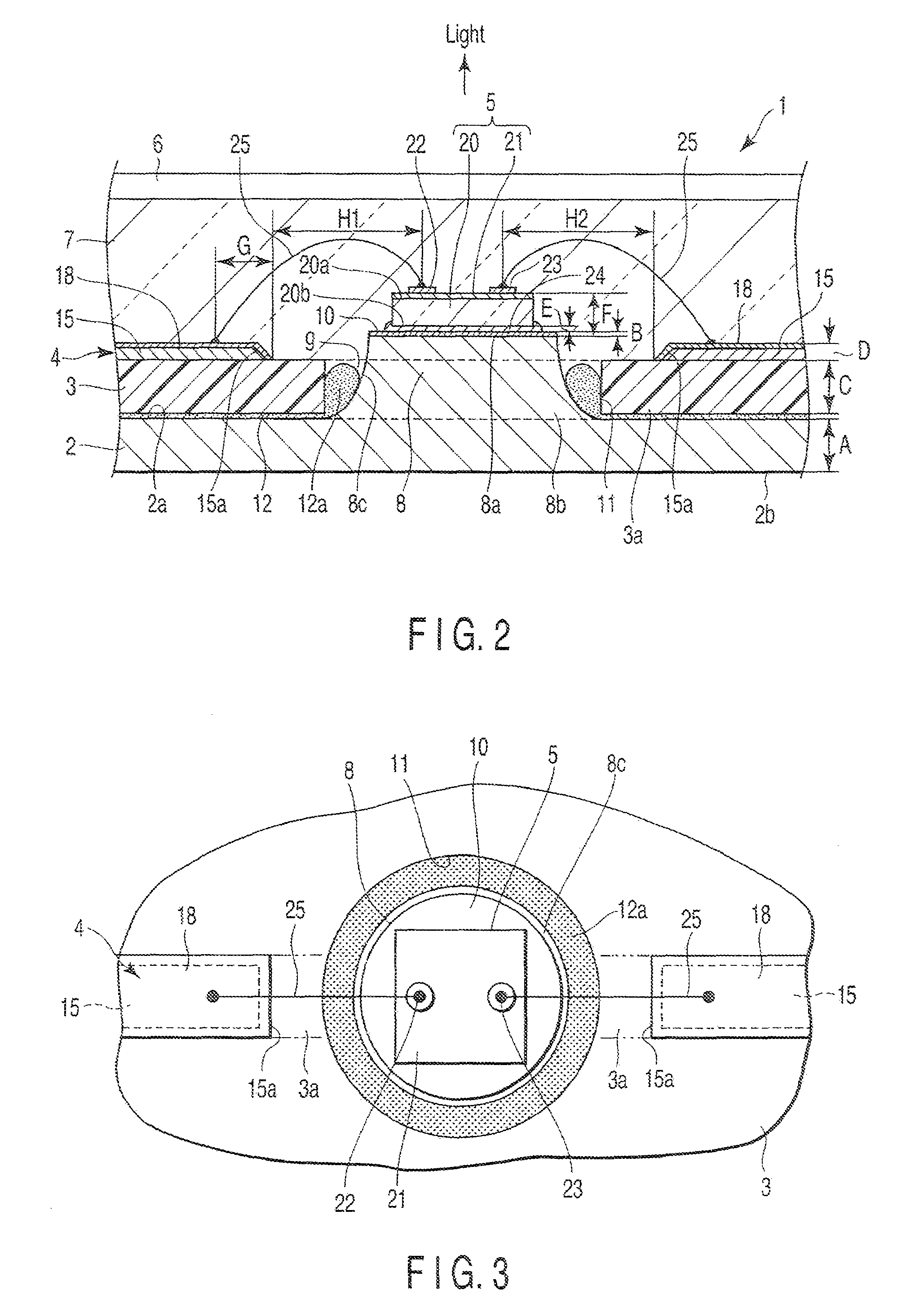
[0079]FIG. 1 discloses an illumination device 1 which constitutes, for example, an LED package. The illumination device 1 includes a base board 2, an insulator 3, a conductor 4, a plurality of semiconductor light-emitting elements 5, a reflector 6 and a sealing member 7.

[0080]The base board 2 has, for example, a rectangular shape in order to obtain a light emission area that is required by the illumination device 1. The material of the base board 2 should preferably be a metal with good heat radiation properties, such as copper or an aluminum alloy. As shown in FIG. 2, the base board 2 has a front surface 2a and a back surface 2b which is located opposite to the front surface 2a. A plurality of columnar projection portions 8 are integrally formed on the front surface 2a of the base board 2. The number of projection portions 8 corresponds to the number of semiconductor light-emitting elements 5.

[0081...

second embodiment

[0129]FIG. 6 shows the present invention. The second embodiment differs from the first embodiment with respect to the structure of the reflector 6. In the other structural aspects, the second embodiment is the same as the first embodiment. Thus, in the second embodiment, the structural parts common to those in the first embodiment are denoted by like reference numerals, and a description thereof is omitted.

[0130]As shown in FIG. 6, the reflector has a plurality of reflection holes 31 (only one of them being shown) which are associated with the semiconductor light-emitting elements 5. The semiconductor light-emitting element 5, which is bonded to the projection portion 8 of the base board 2, is individually disposed in the reflection hole 31. The reflection hole 31 is a taper hole with a diameter which gradually increases from the base board 2 in the light-extraction direction. The sealing member 7 is filled in each of the reflection holes 31. The sealing member 7 is continuously fil...

third embodiment

[0133]FIG. 7 shows the present invention.

[0134]The third embodiment differs from the first embodiment in that the reflector of the illumination device 1 is dispensed with. In the other respects, the structure of the illumination device 1 of the third embodiment is the same as in the first embodiment.

[0135]In the third embodiment, the semiconductor light-emitting element 5, which is bonded to the projection portion 8 of the base board 2, is individually sealed by a sealing member 41. The sealing member 41 is formed by dispensing a non-solidified resin on each of the semiconductor light-emitting element 5 from a dispenser (not shown). The non-solidified resin, after dispensed from the dispenser, is solidified in a hemispherical shape. The sealing member 41 includes a phosphor. The phosphor is uniformly dispersed in the sealing member 41. Further, the sealing member 41 is continuously filled in the gap g between the through hole 11 of the insulator 3 and the outer peripheral surface 8c...


PUM


Abstract

An illumination device includes a base board, an insulator, a conductor, a plurality of semiconductor light-emitting elements and a light-transmissive sealing member. The base board includes a surface and projection portions. The projection portion is formed to become gradually thicker from its end toward the surface of the base board. The insulator is formed on the surface. The conductor is formed on the insulator. The semiconductor light-emitting elements are mounted on the projection portions. The semiconductor light-emitting elements are electrically connected to the conductor via connection members. The sealing member covers the insulator, the projection portions, the semiconductor light-emitting elements and the connection members.

Description

CROSS-REFERENCE TO RELATED APPLICATIONS[0001]This application is based upon and claims the benefit of priority from prior Japanese Patent Applications No. 2006-324606, filed Nov. 30, 2006; No. 2006-353468, filed Dec. 27, 2006; No. 2007-075637, filed Mar. 22, 2007; No. 2007-075638, filed Mar. 22, 2007; No. 2007-082882, filed Mar. 27, 2007; and No. 2007-250227, filed Sep. 26, 2007, the entire contents of all of which are incorporated herein by reference.BACKGROUND OF THE INVENTION[0002]1. Field of the Invention[0003]The present invention relates to an illumination device which uses, as light sources, a plurality of semiconductor light-emitting elements such as light-emitting diode chips.[0004]2. Description of the Related Art[0005]Jpn. Pat. Appln. KOKAI Publication No. 2002-94122 discloses an illumination device in which a plurality of light-emitting diode chips are arranged on a base board. In this illumination device, in order to achieve enhancement of light emission efficiency, an ...

Claims


Application Information

Patent Timeline
Patent Type & Authority Patents(United States)
IPC IPC(8): F21V29/00H01L33/62H01L33/64
CPCH05K1/0203H01L33/60H01L2224/48227H01L33/642H01L2224/32188H01L2224/48091H01L2224/73265H01L2924/01012H01L2924/01078H01L2924/3025H05K3/0061H05K2201/09054H05K2201/10106H01L33/62H01L2224/48465H01L2224/32245H01L2924/01019H01L2924/00014H01L2924/00H01L2224/45099
Inventor SANPEI, TOMOHIROHAYASHIDA, YUMIKOIZUMI, MASAHIROOTANI, KIYOSHIHONDA, YUTAKANOGI, SHINJI
Owner TOSHIBA LIGHTING & TECH CORP
Why Eureka
Try Eureka