Organic light emitting display device

a display device and light-emitting technology, applied in the field of organic light-emitting display devices, can solve the problems of low transmittance of the entire transparent display device, low transmittance of wires, so as to prevent or reduce the distortion of an image transmitted, improve the transmittance of external light, and eliminate or substantially eliminate light-scattering during image display

Active Publication Date: 2015-08-18
SAMSUNG DISPLAY CO LTD
View PDF16 Cites 4 Cited by
  • Summary
  • Abstract
  • Description
  • Claims
  • Application Information

AI Technical Summary

Benefits of technology

[0012]According to an aspect of embodiments of the present invention, in an organic light emitting display device, transparent transmissive areas are formed by improving the transmissivity of the transmissive areas, and dual emission occurs.
[0013]According to another aspect of embodiments of the present invention, a transparent organic light emitting display device prevents or reduces distortion of an image transmitted therethrough by preventing or substantially preventing light from scattering during image display.
[0039]According to an aspect of embodiments of the present invention, a transparent organic light emitting display device may be manufactured by improving the transmissivity of external light and to allow dual emission to occur in the transparent organic light emitting display device.
[0040]According to another aspect of embodiments of the present invention, a transparent organic light emitting display device is capable of preventing or reducing distortion of an image transmitted therethrough by eliminating or substantially eliminating light-scattering during image display.

Problems solved by technology

However, the patterns of organic light emitting diodes, TFTs, and wires do not have a high transmissivity, and the spaces between the patterns are not very high.
Thus, the transmissivity of the entire transparent display device is typically not great.
Therefore, a distorted image may be transmitted to the user due to the patterns of organic light emitting diodes, TFTs, and wires.
However, in this case, the dual-sided light emitting display device cannot be embodied as a transparent display device.

Method used


Image

  • Organic light emitting display device
  • Organic light emitting display device
  • Organic light emitting display device

Examples


Embodiment Construction

[0056]In the following detailed description, some exemplary embodiments of the present invention are shown and described, by way of illustration. As those skilled in the art would realize, the described embodiments may be modified in various different ways, all without departing from the spirit or scope of the present invention. Accordingly, the drawings and description are to be regarded as illustrative in nature and not restrictive.

[0057]As used herein, the term “and / or” includes any and all combinations of one or more of the associated listed items. Expressions such as “at least one of,” when preceding a list of elements, modify the entire list of elements and do not modify the individual elements of the list.

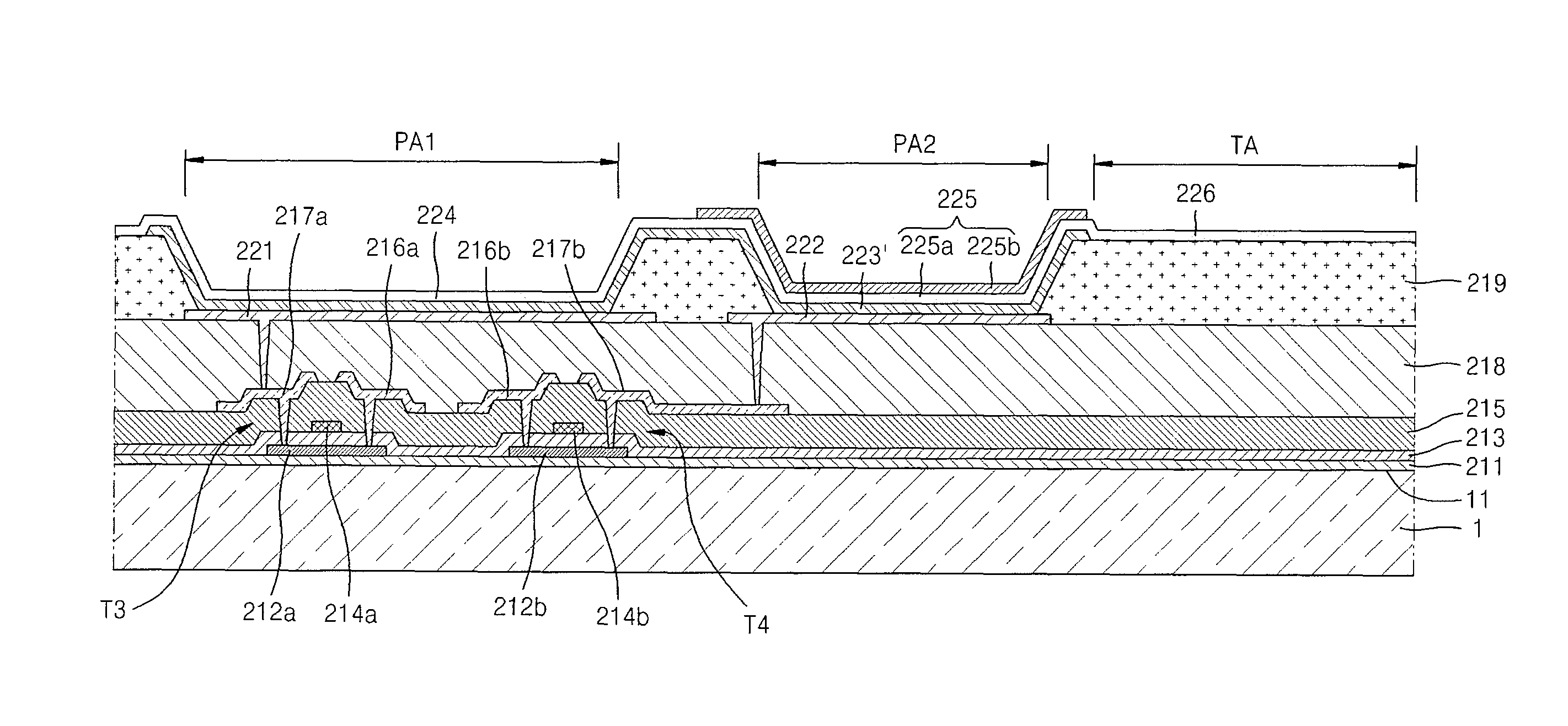
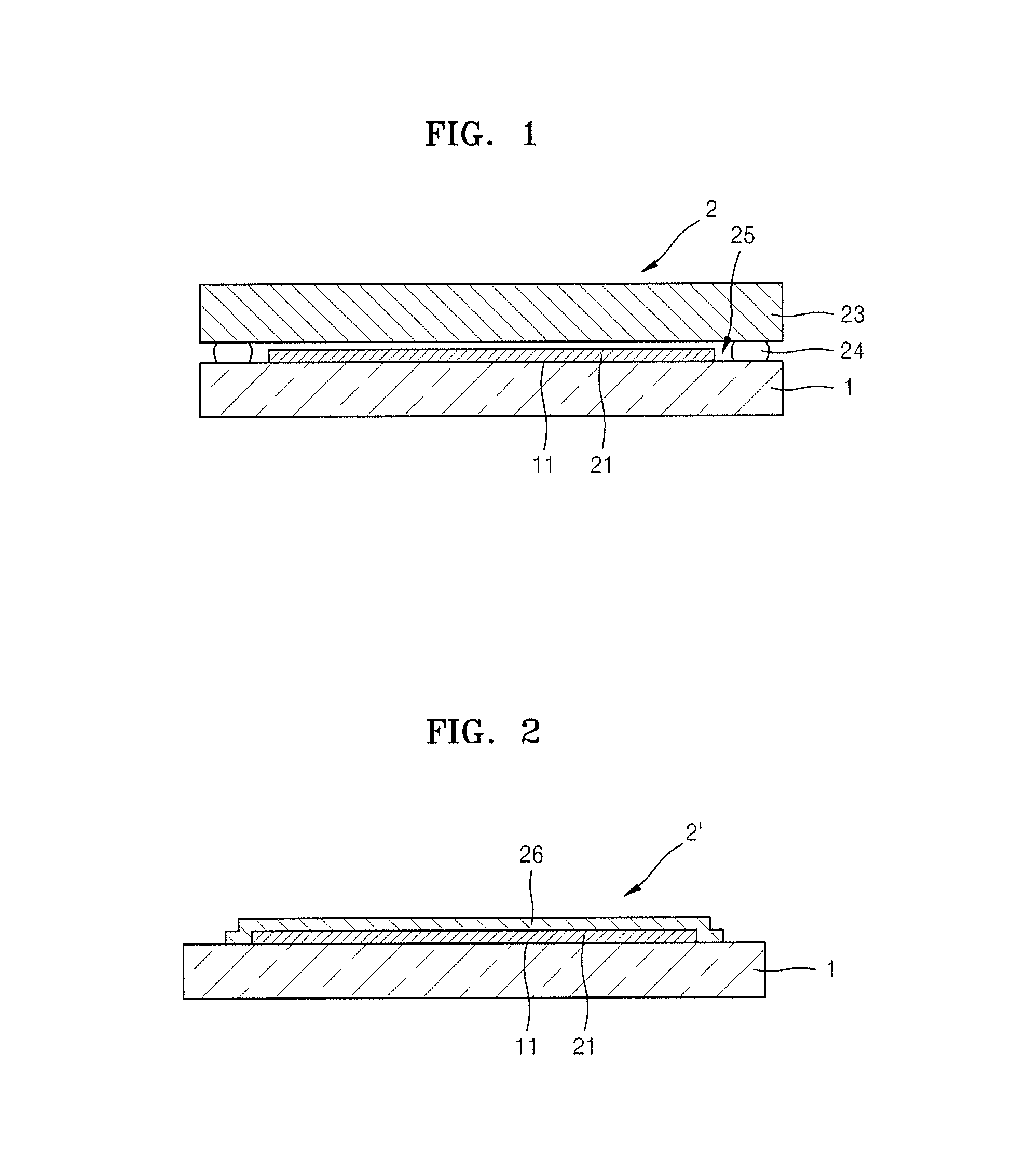
[0058]FIG. 1 is a cross-sectional view of an organic light emitting display device 2 according to an embodiment of the present invention. Referring to FIG. 1, the organic light emitting display device 2 includes an organic emission unit 21 formed on a first surface 11 of a s...


PUM


Abstract

An organic light emitting display device including: a first emission area including a first organic light emitting diode; a second emission area arranged adjacent to the first emission area and not overlapping with the first emission area, the second emission area including a second organic light emitting diode; a pixel circuit unit electrically connected to the first organic light emitting diode and the second organic light emitting diode; and a transmissive area adjacent to the first and second emission areas and not overlapping with the first and second emission areas, the transmissive area configured to transmit external light therethrough.

Description

CROSS-REFERENCE TO RELATED APPLICATION[0001]This application claims priority to and the benefit of Korean Patent Application No. 10-2012-0006809, filed on Jan. 20, 2012 in the Korean Intellectual Property Office, the entire content of which is incorporated herein by reference.BACKGROUND[0002]1. Field[0003]Aspects of embodiments of the present invention relate to organic light emitting display devices.[0004]2. Description of the Related Art[0005]Organic light emitting display devices generally have wide viewing angles, high contrast ratios, short response times, and reduced power consumption, and thus may be used across a variety of applications, such as personal portable devices (e.g., MP3 players and mobile phones), or large-screen displays (e.g., television sets).[0006]An organic light emitting display device has self-emitting characteristics, and weight and thickness of the organic light emitting display device can be reduced since the organic light emitting display device does n...

Claims


Application Information

Patent Timeline
Patent Type & Authority Patents(United States)
IPC IPC(8): H01L29/08H01L27/32H01L29/04
CPCH01L27/326H01L2251/5323Y02E10/50H10K59/128H10K59/1213H10K59/131H10K50/818H10K50/828H10K50/852H10K2102/3031H01L31/0468H01L23/53214H01L23/53219H01L23/53233H01L2924/13069H10K59/121H10K50/30H10K50/816H10K59/123H10K2102/00H10K2102/351
Inventor CHUNG, JIN-KOOCHOI, JUN-HOKIM, SEONG-MIN
Owner SAMSUNG DISPLAY CO LTD
Why Eureka
Try Eureka