
Phosphor substrate, display device, and electronic apparatus

a technology of display device and phosphor substrate, which is applied in the direction of lighting and heating apparatus, semiconductor devices for light sources, instruments, etc., can solve the problems of narrow viewing angle of liquid crystal displays, low image recognition performance when viewed from an oblique direction, and difficulty in increasing definition and siz

Active Publication Date: 2015-11-10
SHARP KK
View PDF14 Cites 21 Cited by
  • Summary
  • Abstract
  • Description
  • Claims
  • Application Information

AI Technical Summary

Benefits of technology

[0033]According to aspects of the present invention, provided are a phosphor substrate capable of sufficiently outputting fluorescence emitted from a phosphor layer to the outside, a display device, and an electronic apparatus.

Problems solved by technology

However, liquid crystal displays have narrow viewing angles and low image recognition performance when viewed from an oblique direction, compared with conventional cathode ray tube displays.
To achieve full-color display, RGB light-emitting layers are required to be patterned by mask deposition, thus causing difficulty in increasing the definition and the size.

Method used


Image

  • Phosphor substrate, display device, and electronic apparatus
  • Phosphor substrate, display device, and electronic apparatus
  • Phosphor substrate, display device, and electronic apparatus

Examples


first embodiment

[First Embodiment]

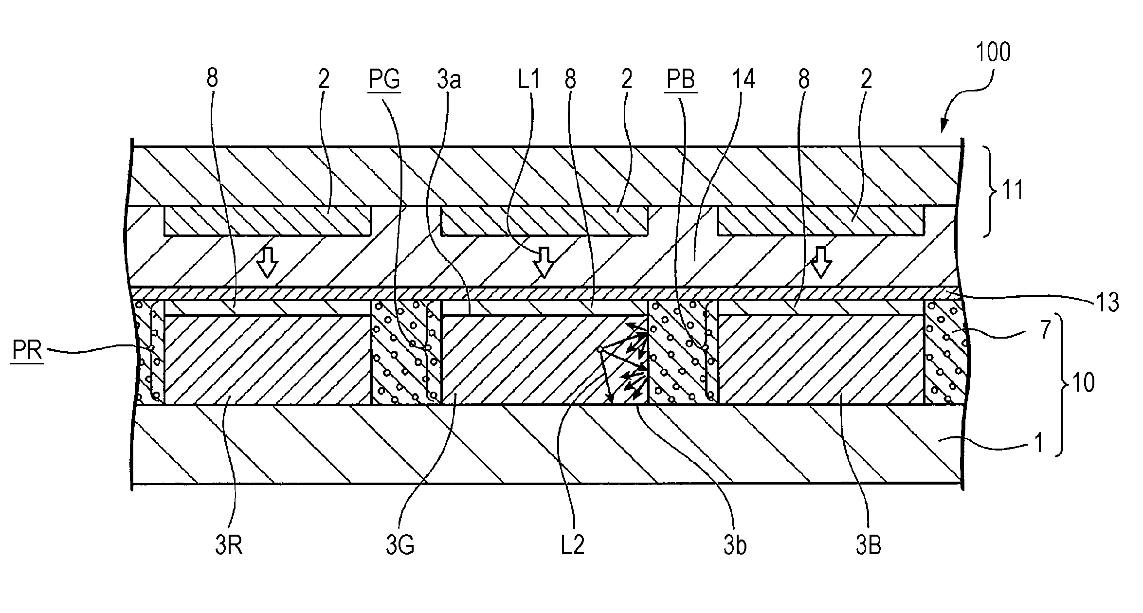
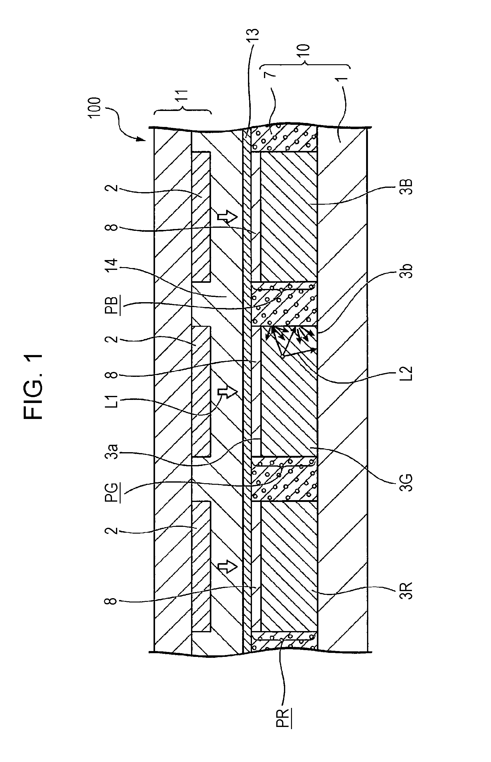
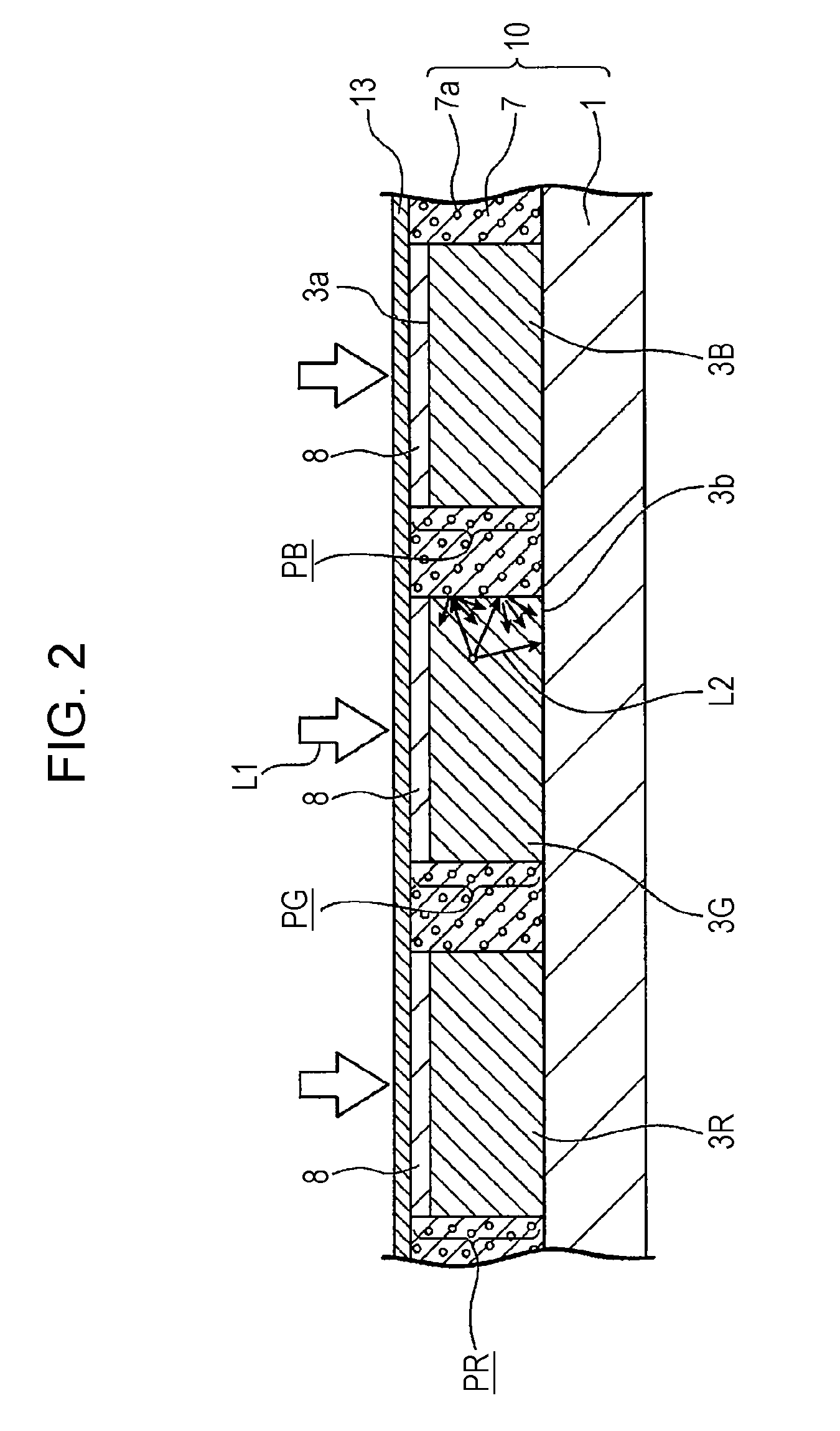
[0079]FIG. 1 is a schematic cross-sectional view of a display device 100 according to a first embodiment.

[0080]The display device 100 includes a phosphor substrate 10, a substrate 13, a light source 11, and an adhesive layer 14. The substrate 13 is provided between the phosphor substrate and the light source 11. The light source 11 includes light-emitting elements 2. Excitation light L1 to be incident on the phosphor substrate 10 is emitted from the light-emitting elements 2. The adhesive layer 14 bonds the light source 11 and the phosphor substrate 10. A common ultraviolet curable resin, a thermosetting resin, or the like may be used for the adhesive layer.

[0081]In the case where a light source is directly disposed on the phosphor substrate 10, the adhesive layer 14 may be arranged at a portion which is located at the periphery of the phosphor substrate 10 and the light source 11 and which is located between the phosphor substrate 10 and the light source 11, and a...

second embodiment

[Second Embodiment]

[0213]A second embodiment of the present invention will be described below with reference to FIGS. 10 and 11.

[0214]A display device according to this embodiment has the same basic structure as the first embodiment. The structure of the partition is different from the first embodiment. Thus, in this embodiment, the description of the basic structure of the display device is omitted, and only the partition will be described.

[0215]FIG. 10 is a schematic cross-sectional view of a display device 100A according to the second embodiment.

[0216]In the first embodiment, the partition 7 includes the light-scattering particles 7a dispersed therein. In contrast, a partition 17 according to this embodiment, portions of the partition 17 (side faces of the partition 17) in contact with the phosphor layers 3R, 3G, and 3B have an uneven shape as illustrated in FIG. 10. The remaining components are the same as the first embodiment. The partition 17 is composed of a resin. The partit...

third embodiment

[Third Embodiment]

[0221]A third embodiment of the present invention will be described below with reference to FIG. 12.

[0222]A display device 100B according to this embodiment has the same basic structure as the first embodiment, except that color filters 4 are disposed between the substrate 1 and the phosphor layers 3 and that black layers 5 and 6 are disposed on the partition 7. Thus, in this embodiment, the description of the basic structure of the display device 100B is omitted.

[0223]FIG. 12 is a schematic cross-sectional view of the display device 100B according to the third embodiment.

[0224]In the display device 100B according to this embodiment, a red color filter 4R is disposed between the substrate 1 and the red phosphor layer 3R. A green color filter 4G is disposed between the substrate 1 and the green phosphor layer 3G. A blue color filter 4B is disposed between the substrate 1 and the blue phosphor layer 3B. Thereby, it is possible to improve the chromaticity.

[0225]A firs...


PUM

PropertyMeasurementUnit
particle sizeaaaaaaaaaa
emission peakaaaaaaaaaa

Abstract

A phosphor substrate (10) includes a substrate (1), phosphor layers (3R, 3G, and 3B) which are disposed on the substrate (1) and which emit fluorescences (L2) using incident excitation light (L1), and a partition (7) surrounding side faces of the phosphor layers (3R, 3G, and 3B), in which at least portions of the partition (7) in contact with the phosphor layers (3R, 3G, and 3B) have light-scattering properties.

Description

CROSS REFERENCE TO RELATED APPLICATIONS[0001]This is a U.S. National Phase patent application of PCT / JP2012 / 069836, filed Aug. 3, 2012, which claims priority to Japanese patent application no. JP 2011-171767, filed Aug. 5, 2011, each of which is hereby incorporated by reference in the present disclosure in its entirety.TECHNICAL FIELD[0002]The present invention relates to a phosphor substrate, a display device, and an electronic apparatus.BACKGROUND ART[0003]In recent years, displays mounted on television sets, personal computers, information terminal assistants, and so forth have been increasingly required to have higher performance. There have been advances in the research and development of various types of display devices, such as cathode ray tube displays, liquid crystals, plasma displays (PDPs), and organic EL displays. In particular, liquid crystal displays are thin and light in weight and thus compose the major portion of a current display market. However, liquid crystal dis...

Claims


Application Information

Patent Timeline
Patent Type & Authority Patents(United States)
IPC IPC(8): G02F1/1335F21K99/00H05B33/14H05B33/10H01L51/52
CPCG02F1/133621F21K9/56H01L51/5268H01L51/5284H05B33/10H05B33/14G02F1/133617G02F2001/133614F21K9/64G02F1/133614H10K50/854H10K50/865
Inventor IWATA, AKIKOKODEN, MITSUHIROKOBAYASHI, YUHKIBESSHO, HISANORISHIBATA, SATOSHI
Owner SHARP KK
Learn More