Analogue to digital conversion device

a conversion device and digital technology, applied in the field of analog to digital (a/d) conversion devices, can solve the problems of difficult detection of high frequency components, difficulty in following and adapting the period of receiving a/d conversion data by the subtraction unit, and the conventional structure of the a/d conversion device not performing a correct a/d conversion operation, etc., to avoid the operation speed of analogue, improve the structure of the analogue to digital conversion device, and improve the effect of high frequency

Active Publication Date: 2016-01-26
DENSO CORP
View PDF6 Cites 0 Cited by
  • Summary
  • Abstract
  • Description
  • Claims
  • Application Information

AI Technical Summary

Benefits of technology

[0012]Because the analogue to digital conversion device having the structure previously described has no subtraction unit, it is possible to avoid the operation speed of the analogue to digital conversion device from being limited and reduced by an operation speed of the subtraction device. That is, the improved structure of the analogue to digital conversion device makes it possible to generate data items which are m times the number of data items generated by the generation speed of the analogue to digital conversion section. Further, because a period for counting the number of the delay units through which pulse signals have passed becomes 1 / m times the period of the sampling signal, it is possible for the analogue to digital conversion data to contain more high frequency signal components.

Problems solved by technology

However, because the conventional technique previously described requires an additional subtraction unit, it becomes difficult for the subtraction unit to follow and adapt a period of receiving A / D conversion data when the operation of the A / D conversion device operates at a high speed (for example, at a GHz speed).
This introduces that the A / D conversion device having the conventional structure does not perform a correct A / D conversion operation.
Further, in the conventional technique of continuously performing the operation of the pulse delay circuit and the pulse loop counter without any resetting process, because the period of the sampling signal and the period of counting the number of the delay units through which the pulse signals have passed have the same value, it is difficult to detect a high frequency component, which is higher than a frequency of the sampling frequency, to the A / D conversion data.

Method used


Image

  • Analogue to digital conversion device
  • Analogue to digital conversion device
  • Analogue to digital conversion device

Examples


Embodiment Construction

[0017]Hereinafter, various embodiments of the present invention will be described with reference to the accompanying drawings. In the following description of the various embodiments, like reference characters or numerals designate like or equivalent component parts throughout the several diagrams.

Exemplary Embodiment

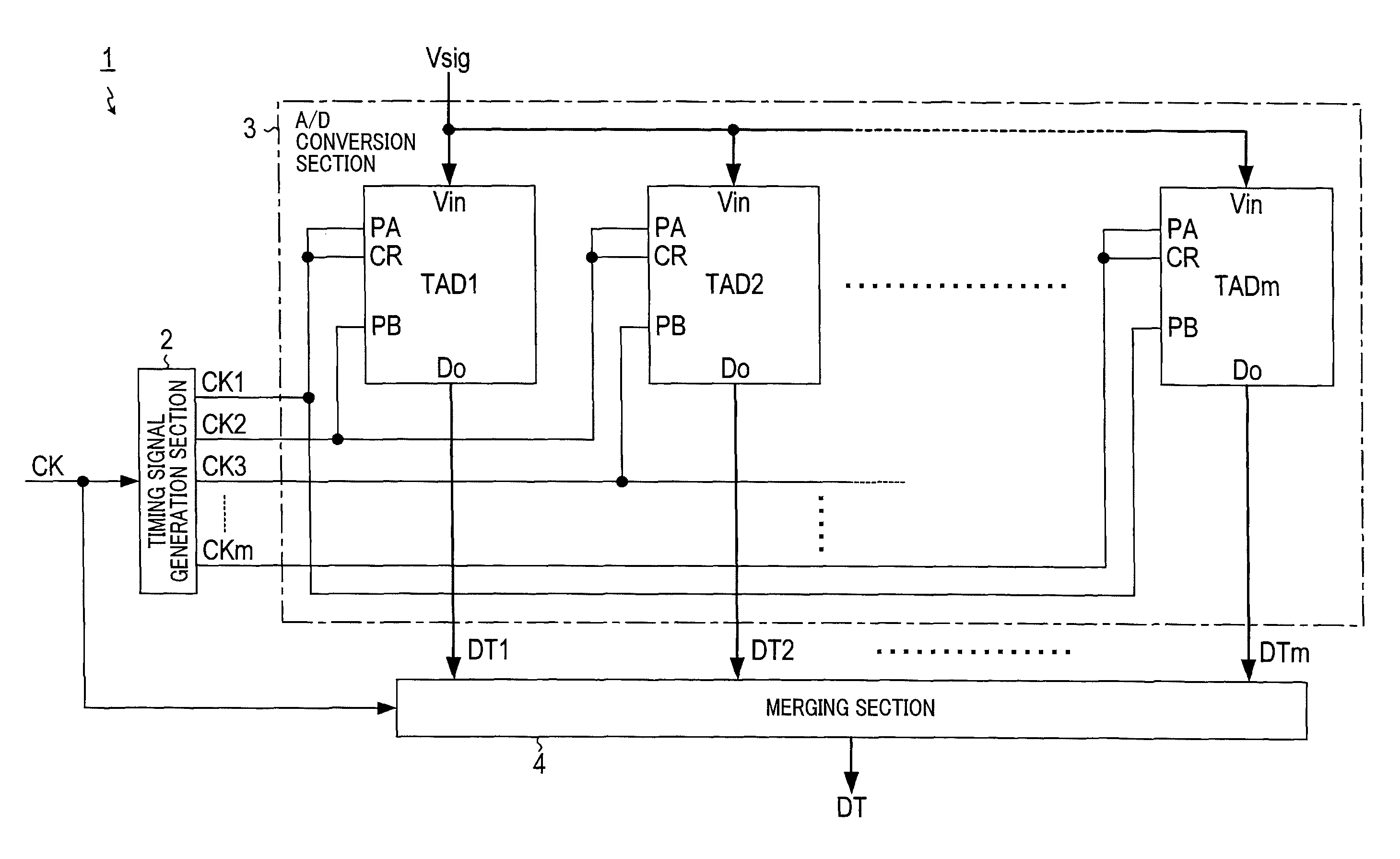
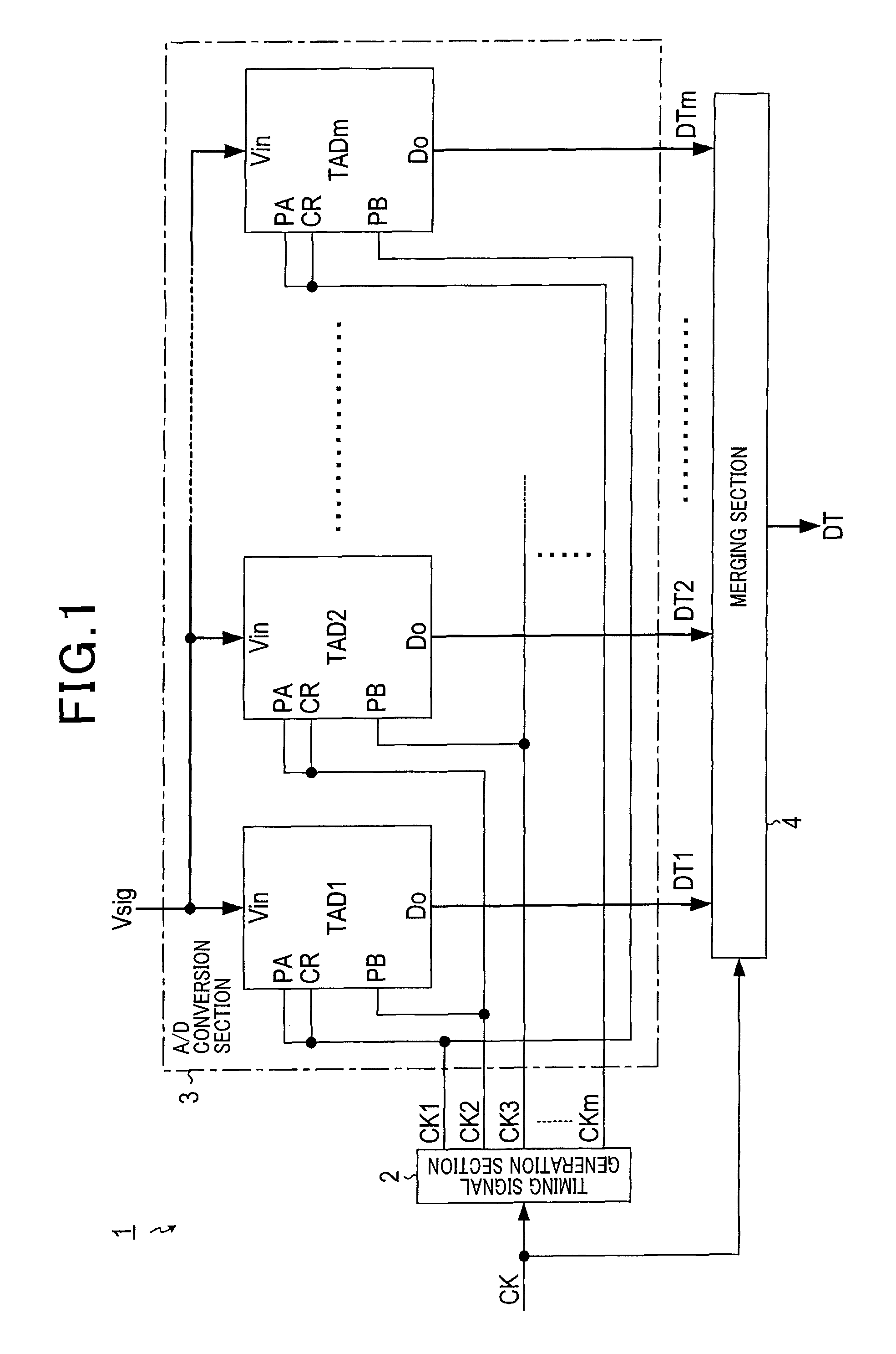
[0018]A description will be given of a structure and operation of an analogue to digital (A / D) conversion device 1 according to the exemplary embodiment. FIG. 1 is a block diagram showing an overall structure of the A / D conversion device 1 according to the exemplary embodiment. As shown in FIG. 1, the A / D conversion device 1 is equipped with a timing signal generation section 2 and an A / D conversion section 3, and a merging section 4.

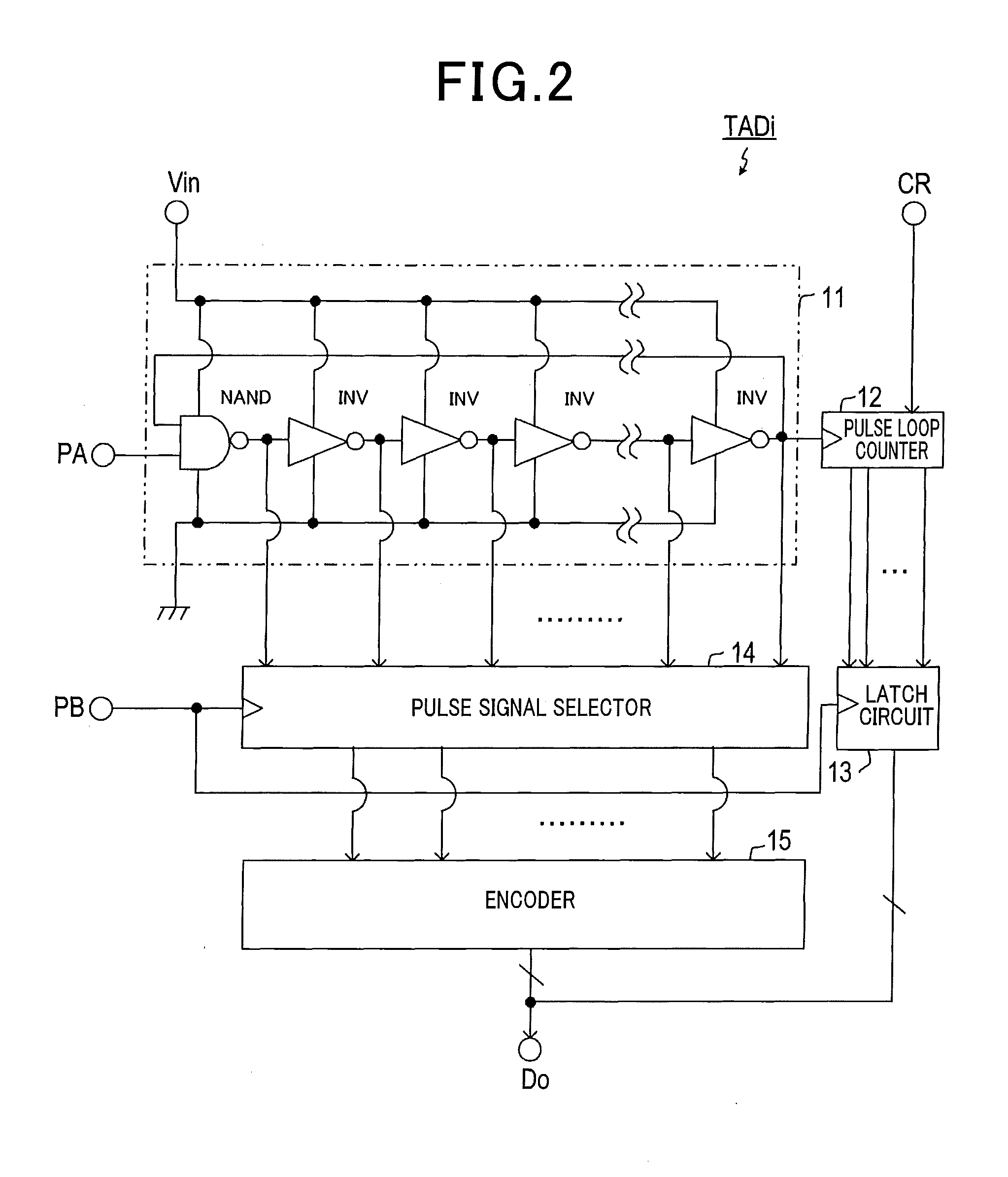
[0019]The timing signal generation section 2 generates m timing signals CKi (i=1, 2, . . . and m), i.e., timing signals CK1 to CKm (m=2n) having a division period. The division period is obtained by dividing a clock signal CK by n (n is an ...


PUM


Abstract

An A / D conversion device has an A / D conversion section including A / D conversion units. Each A / D conversion unit has a pulse delay circuit including delay units connected in daisy chain to form a ring delay line. Each delay unit delays a pulse signal by a delay time corresponding to an input voltage. The A / D conversion section counts the number of pulse signals that passed through the delay units during a period counted from a timing when a start signal is switched to an activation level from a non-activation level at a timing when a sampling signal is received. When each two successive timing signals CKi (i=1, 2, . . . and m) have a same specific period. The each two successive timing signals have a different phase shifted by 1 / m of the specific period. Each A / D conversion unit receives the timing signal CK1 as the start signal, and the timing signal CKi+1 (CKm+1=CK1) as the sampling signal.

Description

CROSS-REFERENCE TO RELATED APPLICATION[0001]This application is related to and claims priority from Japanese Patent Application No. 2014-69764 filed on Mar. 28, 2014, the contents of which are hereby incorporated by reference.BACKGROUND OF THE INVENTION[0002]1. Field of the Invention[0003]The present invention relates to analogue to digital (A / D) conversion devices equipped with a plurality of delay units arranged in multiple stages, and each of the delay units is capable of delaying a received pulse signal by a delay time which corresponds to an input voltage.[0004]2. Description of the Related Art[0005]There have been used various types of analogue to digital (A / D) conversion devices having a conventional structure. For example, a patent document, Japanese patent laid open publication No. H05-259907 has disclosed a conventional A / D conversion device equipped with a pulse delay circuit. The pulse delay circuit is comprised of a plurality of delay units. The delay units are arranged...

Claims


Application Information

Patent Timeline
Patent Type & Authority Patents(United States)
IPC IPC(8): H03M1/60H03M1/14H03M1/62
CPCH03M1/146H03M1/60H03M1/62H03M1/502
Inventor TERAZAWA, TOMOHITO
Owner DENSO CORP
Why Eureka
Try Eureka