Method of fabricating a light emitting diode display with integrated defect detection test

a technology of light emitting diodes and defect detection, applied in the field of display systems, can solve the problems of contaminated micro led devices, micro led devices missing, micro led devices being damaged, etc., and achieve the effect of reducing the probability of correlated defects being transferred

Active Publication Date: 2016-02-02
APPLE INC
View PDF99 Cites 117 Cited by
  • Summary
  • Abstract
  • Description
  • Claims
  • Application Information

AI Technical Summary

Benefits of technology

The patent describes a way to transfer micro LED devices from a carrier substrate to a display substrate using electrostatic force. The first and second arrays of micro LED devices can be transferred from different areas of the carrier substrate or from different carriers to reduce the chance of defects being transferred to the same subpixel. The use of separate electrostatic transfer heads for each micro LED device allows for more precise and reliable transfer. Overall, the technique provides a more efficient and reliable way to transfer micro LED devices during the manufacturing process.

Problems solved by technology

For example, the irregularities can be missing micro LED devices, defective micro LED devices, and contaminated micro LED devices.

Method used


Image

  • Method of fabricating a light emitting diode display with integrated defect detection test
  • Method of fabricating a light emitting diode display with integrated defect detection test
  • Method of fabricating a light emitting diode display with integrated defect detection test

Examples


Embodiment Construction

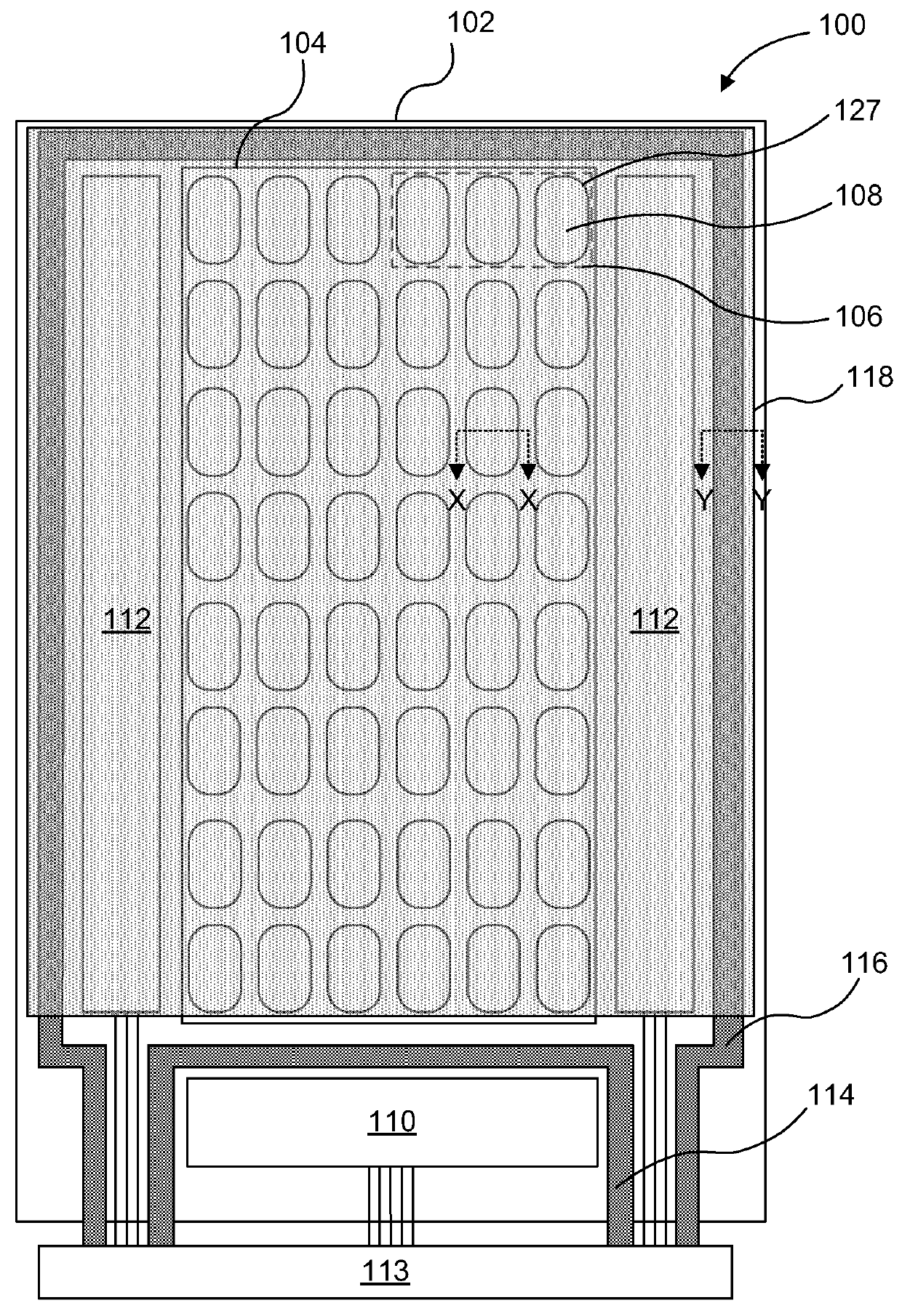
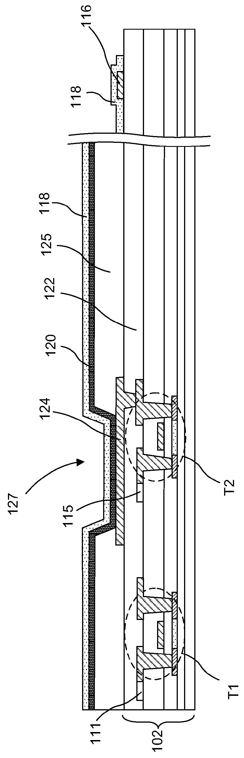
[0047]Embodiments of the present invention relate to display systems. More particularly embodiments of the present invention relate to a display with a redundancy scheme of light emitting diodes.

[0048]In one aspect, embodiments of the invention describe an active matrix display panel including wafer-based emissive micro LED devices. A micro LED device combines the performance, efficiency, and reliability of wafer-based LED devices with the high yield, low cost, mixed materials of thin film electronics used to form AMOLED backplanes. The terms “micro” device or “micro” LED structure as used herein may refer to the descriptive size of certain devices or structures in accordance with embodiments of the invention. As used herein, the terms “micro” devices or structures are meant to refer to the scale of 1 to 100 μm. However, it is to be appreciated that embodiments of the present invention are not necessarily so limited, and that certain aspects of the embodiments may be applicable to l...


PUM


Abstract

A display panel and method of manufacture are described. In an embodiment, a display substrate includes a pixel area and a non-pixel area. An array of subpixels and corresponding array of bottom electrodes are in the pixel area. An array of micro LED devices are bonded to the array of bottom electrodes. One or more top electrode layers are formed in electrical contact with the array of micro LED devices. In one embodiment a redundant pair of micro LED devices are bonded to the array of bottom electrodes. In one embodiment, the array of micro LED devices are imaged to detect irregularities.

Description

BACKGROUND[0001]1. Field[0002]Embodiments of the present invention relate to display systems. More particularly embodiments of the present invention relate to display systems incorporating micro light emitting diodes.[0003]2. Background Information[0004]Flat panel displays are gaining popularity in a wide range of electronic devices. Common types of flat panel displays include active matrix displays and passive matrix displays. Each pixel in an active matrix display panel is driven by active driving circuitry, while each pixel in a passive matrix display panel does not use such driving circuitry. High-resolution color display panels, such as modern computer displays, smart phones and televisions typically use an active matrix display panel structure for better image quality.[0005]One kind of display panel that is finding commercial application is an active matrix organic light emitting diode (AMOLED) display panel. FIG. 1 is a top view illustration of a top emission AMOLED display p...

Claims


Application Information

Patent Timeline
Patent Type & Authority Patents(United States)
IPC IPC(8): H01L51/50G09G3/00H01L23/00H01L21/683
CPCH01L51/50G09G3/006H01L21/6835H01L24/24H01L24/75H01L24/82H01L24/83H01L24/97H01L24/32H01L2221/68368H01L2221/68381H01L2224/2401H01L2224/2405H01L2224/245H01L2224/24011H01L2224/24137H01L2224/24227H01L2224/29005H01L2224/29109H01L2224/29111H01L2224/29113H01L2224/29118H01L2224/29124H01L2224/29139H01L2224/29144H01L2224/29147H01L2224/29155H01L2224/32014H01L2224/32057H01L2224/32237H01L2224/32503H01L2224/759H01L2224/7565H01L2224/7598H01L2224/75252H01L2224/75301H01L2224/75725H01L2224/82101H01L2224/82102H01L2224/82104H01L2224/83005H01L2224/8381H01L2224/8383H01L2224/83192H01L2224/83193H01L2224/83203H01L2224/83805H01L2224/83825H01L2224/97H01L2924/12041H01L27/1214G09G3/3208H01L2924/12042H01L2924/12044H01L2924/00014H01L2924/01049H01L2924/0105H01L2924/00012H01L2224/83H01L2924/053H01L2924/0549H01L2924/0543H01L2924/0544H01L2924/0103H01L2924/0781H01L2924/01013H01L2924/01042H01L2924/01022H01L2924/01074H01L2924/01047H01L2924/01079H01L2924/00H01L27/156H10K50/00H10K59/12H10K59/10
Inventor BIBL, ANDREASSAKARIYA, KAPIL V.GRIGGS, CHARLES R.PERKINS, JAMES MICHAEL
Owner APPLE INC
Why Eureka
Try Eureka