Variable inductor and semiconductor device using same

a variable inductor and semiconductor technology, applied in the direction of continuous variable inductance/transformer, inductance without magnetic core, inductance, etc., can solve the problem of increasing the loss of matching circuit, and achieve the effect of efficient chang

Active Publication Date: 2016-04-26
PANASONIC CORP
View PDF17 Cites 1 Cited by
  • Summary
  • Abstract
  • Description
  • Claims
  • Application Information

AI Technical Summary

Benefits of technology

[0037]In the variable inductor of the invention, a loop conductor using a pass-through via that penetrate through a silicon substrate is placed in a layer located lower than a spiral inductor. One end of the loop conductor is opened or short-circuited by a switch, thereby controlling an induced current flowing through the loop conductor. Thereby, an inductance value can efficiently be changed at a high frequency band. Accordingly, a variable matching circuit used in a case where matching of a wide band, as in millimeter wave frequency bands, must be controlled, can be configured.

Problems solved by technology

In general, providing a matching circuit with a lumped parameter poses a problem of a band being narrowed by a self-resonant frequency of inductance or capacitance.
However, using the varactor or the switch at millimeter wave frequency bands causes a problem of an increase in loss of the matching circuit.

Method used


Image

  • Variable inductor and semiconductor device using same
  • Variable inductor and semiconductor device using same
  • Variable inductor and semiconductor device using same

Examples


first embodiment

[0053](First Embodiment)

[0054]A first embodiment of the invention is now described by reference to the drawings.

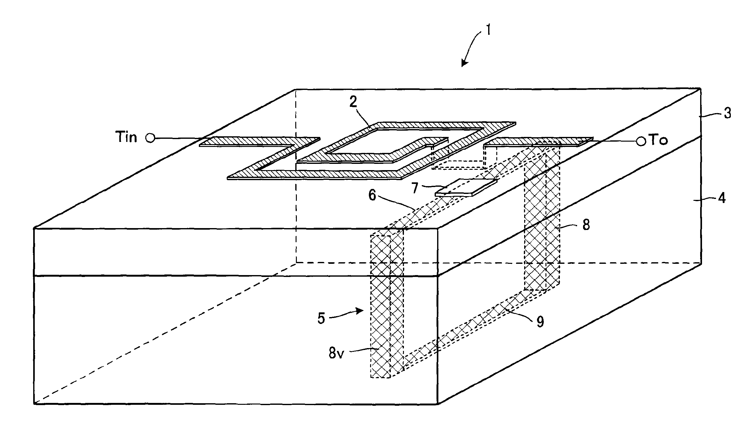
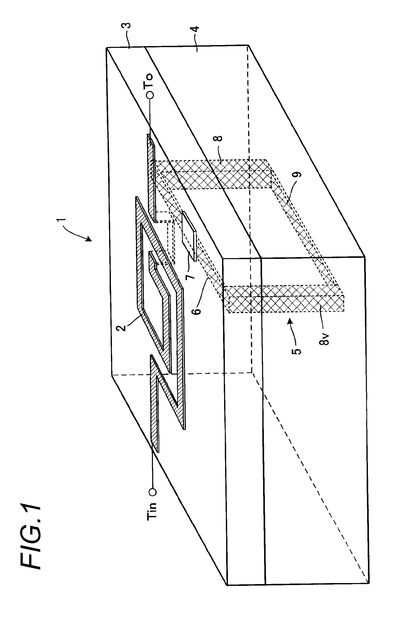
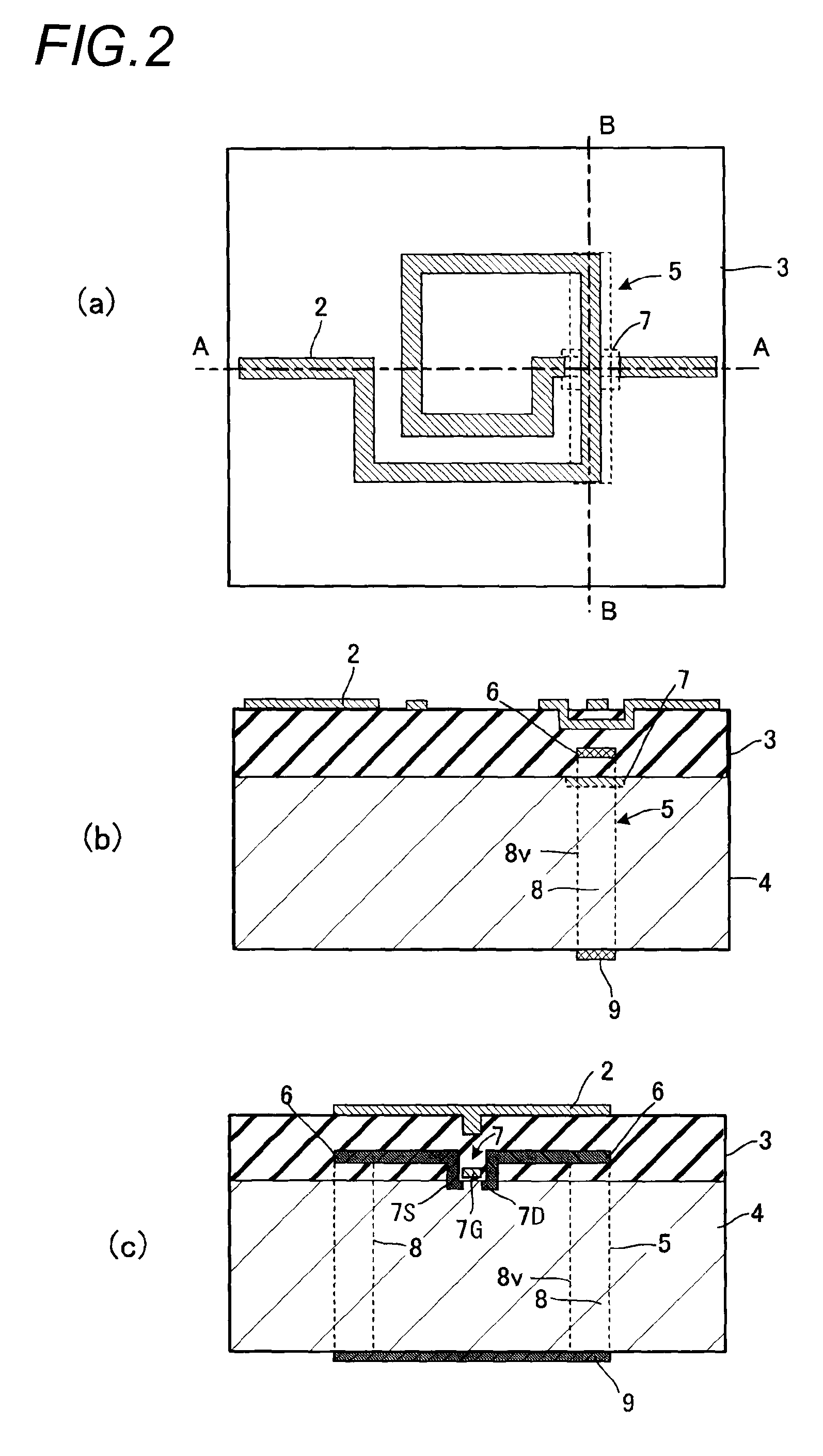
[0055]FIG. 1 is a schematic diagram of a variable inductor of a first embodiment. FIG. 2(a) is a top view of the variable inductor 1; FIG. 2(b) is a cross sectional view taken along line A-A; and FIG. 2(c) is a cross sectional view taken along line B-B. FIG. 3 is schematic drawings of a semiconductor integrated circuit device 100 including the variable inductor 1; FIG. 3(a) is an equivalent circuit of the semiconductor integrated circuit device 100, and FIG. 3(b) is a schematic block diagram of the semiconductor integrated circuit device 100.

[0056]As illustrated in FIGS. 3(a) and (b), the variable inductor 1 is populated on a semiconductor integrated circuit board (a silicone substrate 4) on which a CMOS semiconductor element including a transistor 20 or a capacitor 21 is populated, to thus constitute the semiconductor integrated circuit device 100. FIG. 1 and FIGS. 2(a) t...

second embodiment

[0089](Second Embodiment)

[0090]A second embodiment of the invention is now described by reference to the drawings.

[0091]FIG. 4 is a schematic diagram of a variable inductor of a second embodiment. FIG. 5(a) is a top view of the variable inductor 1, and FIG. 5(b) is a cross sectional view taken along line A-A.

[0092]As in the case with the first embodiment, the variable inductor 1 is populated on the semiconductor integrated circuit board (the silicon substrate 4) on which the CMOS semiconductor element including the transistor 20 or the capacitor 21 is populated, thereby making up the semiconductor integrated circuit device 100 (see FIGS. 3(a) and 3(b)). The variable inductor is illustrated in the embodiment, and other element regions are omitted.

[0093]As illustrated in FIG. 5, the variable inductor 1 is made up of the spiral inductor 2 formed over the surface of the silicon substrate 4 serving as a semiconductor substrate; two loop conductors formed in a direction perpendicular to t...

third embodiment

[0103](Third Embodiment)

[0104]A third embodiment of the invention is now described by reference to the drawings. FIG. 6 is a schematic diagram of a variable inductor of the third embodiment.

[0105]As in the case with the first embodiment, the variable inductor 1 is populated on the semiconductor integrated circuit board (the silicon substrate 4) on which the CMOS semiconductor element including the transistor 20 or the capacitor 21 is populated, thereby making up the semiconductor integrated circuit device 100 (see FIGS. 3(a) and 3(b)). The variable inductor is illustrated in the embodiment, and other element regions are omitted.

[0106]As illustrated in FIG. 6, the variable inductor 1 is made up of the spiral inductor 2 formed over the surface of the silicon substrate 4 serving as a semiconductor substrate; four loop conductors formed in a direction perpendicular to the spiral inductor 2, or first through fourth loop conductors 5a through 5d; and first through fourth switches 7a throu...


PUM

PropertyMeasurementUnit
semiconductoraaaaaaaaaa
inductanceaaaaaaaaaa
self-resonant frequencyaaaaaaaaaa

Abstract

A variable inductor includes a spiral inductor, a loop conductor, and a switch for opening or short-circuiting an end of the loop conductor. The loop conductor is formed in a direction perpendicular to the spiral inductor and is used for adjusting the inductance value of the spiral inductor by opening or short-circuiting the end of the loop conductor by the switch.

Description

TECHNICAL FIELD[0001]The invention relates to a variable inductor and a semiconductor device using the same and a technique of controlling an inductance value of an inductor, which makes up a matching circuit, in a semiconductor device that is formed by use of; for instance, CMOS processes, and used at ultrahigh frequency bands, including millimeter wave frequency bands.BACKGROUND ART[0002]Development of an MMIC (monolithic microwave integrated circuit) using CMOS processes has been pursued in a field of wireless communication using millimeter wave frequency bands, and reducing chip's area by providing a matching circuit with a lumped parameter has also been pursued.[0003]In general, providing a matching circuit with a lumped parameter poses a problem of a band being narrowed by a self-resonant frequency of inductance or capacitance.[0004]In a matching circuit using a lumped parameter element, the matching circuit is generally made variable in order to enhance a narrow band characte...

Claims


Application Information

Patent Timeline
Patent Type & Authority Patents(United States)
IPC IPC(8): H01F21/12H01L49/02H01L23/522H01F21/00H01F27/28H01L27/06
CPCH01L23/5227H01L28/10H01F21/005H01F27/2804H01L27/0605H01F2027/2809H01L2924/0002H01L2924/00
Inventor SATO, JUNJIMIZUNO, KOICHIFUJITA, SUGURU
Owner PANASONIC CORP
Why Eureka
Try Eureka