Optoelectronic device and method for manufacturing same

a technology of optoelectronic devices and manufacturing methods, applied in the field of semiconductor microwires or nanowires, can solve the problems of altering the efficiency of the conversion of an electric signal into an electromagnetic radiation or the other, and the growth of nanowires may be disturbed, so as to achieve accurate and uniform control and low cost

Active Publication Date: 2016-05-03
ALEDIA
View PDF12 Cites 3 Cited by
  • Summary
  • Abstract
  • Description
  • Claims
  • Application Information

AI Technical Summary

Benefits of technology

This patent describes a way to accurately and uniformly control the position, geometry, and crystallographic properties of semiconductor microwires or nanowires, and to form them at an industrial scale and at low cost. Additionally, the patent also includes a method to prevent the growth of semiconductor elements on the lateral sides of pads.

Problems solved by technology

However, with the method disclosed in U.S. Pat. No. 7,829,443, the nanowire growth may be disturbed, so that each nanowire might not have a single-crystal structure.
This may cause the forming of defects, especially at grain boundaries, which may alter the efficiency of the conversion of an electric signal into an electromagnetic radiation or the other way.

Method used


Image

  • Optoelectronic device and method for manufacturing same
  • Optoelectronic device and method for manufacturing same
  • Optoelectronic device and method for manufacturing same

Examples


Embodiment Construction

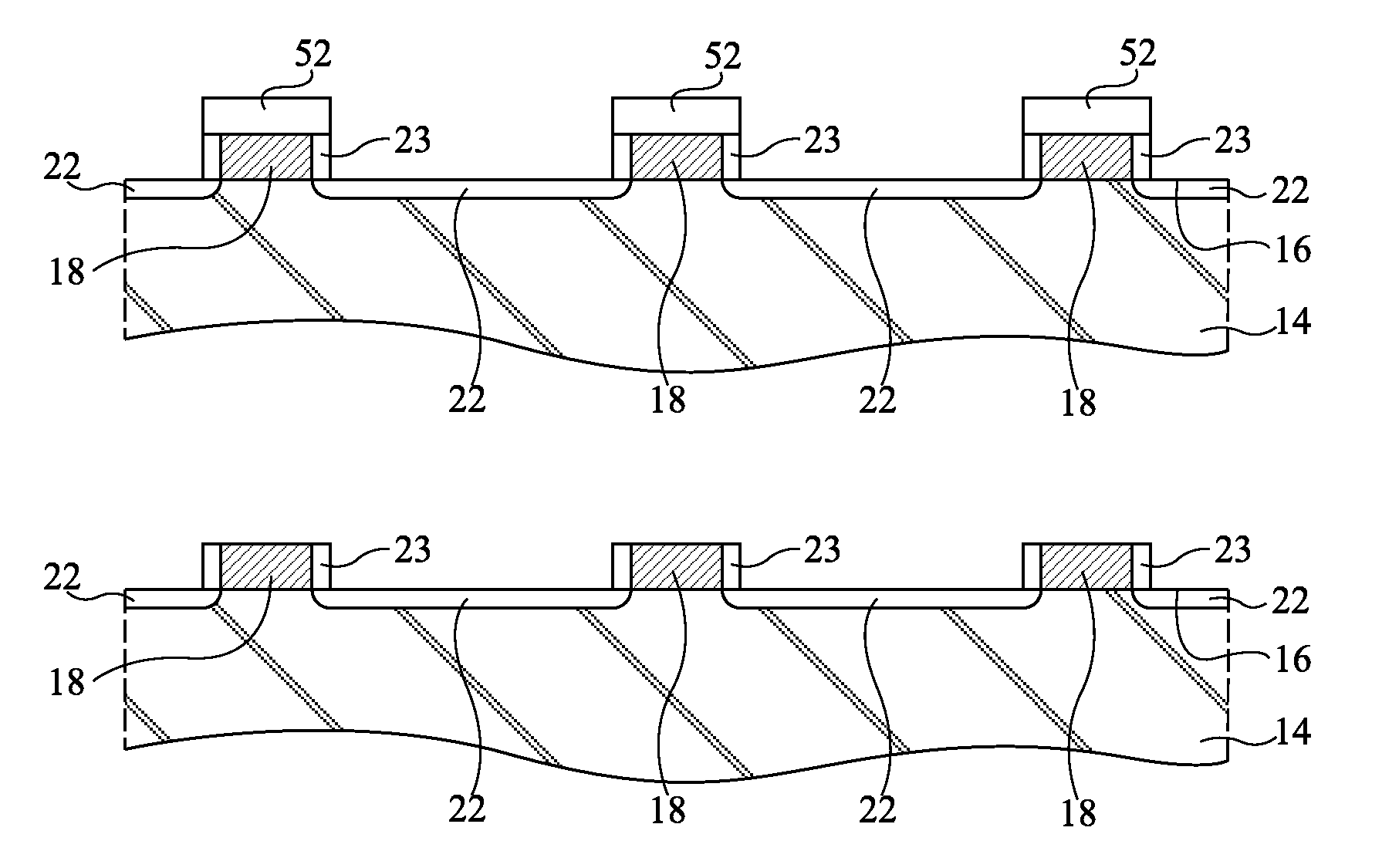
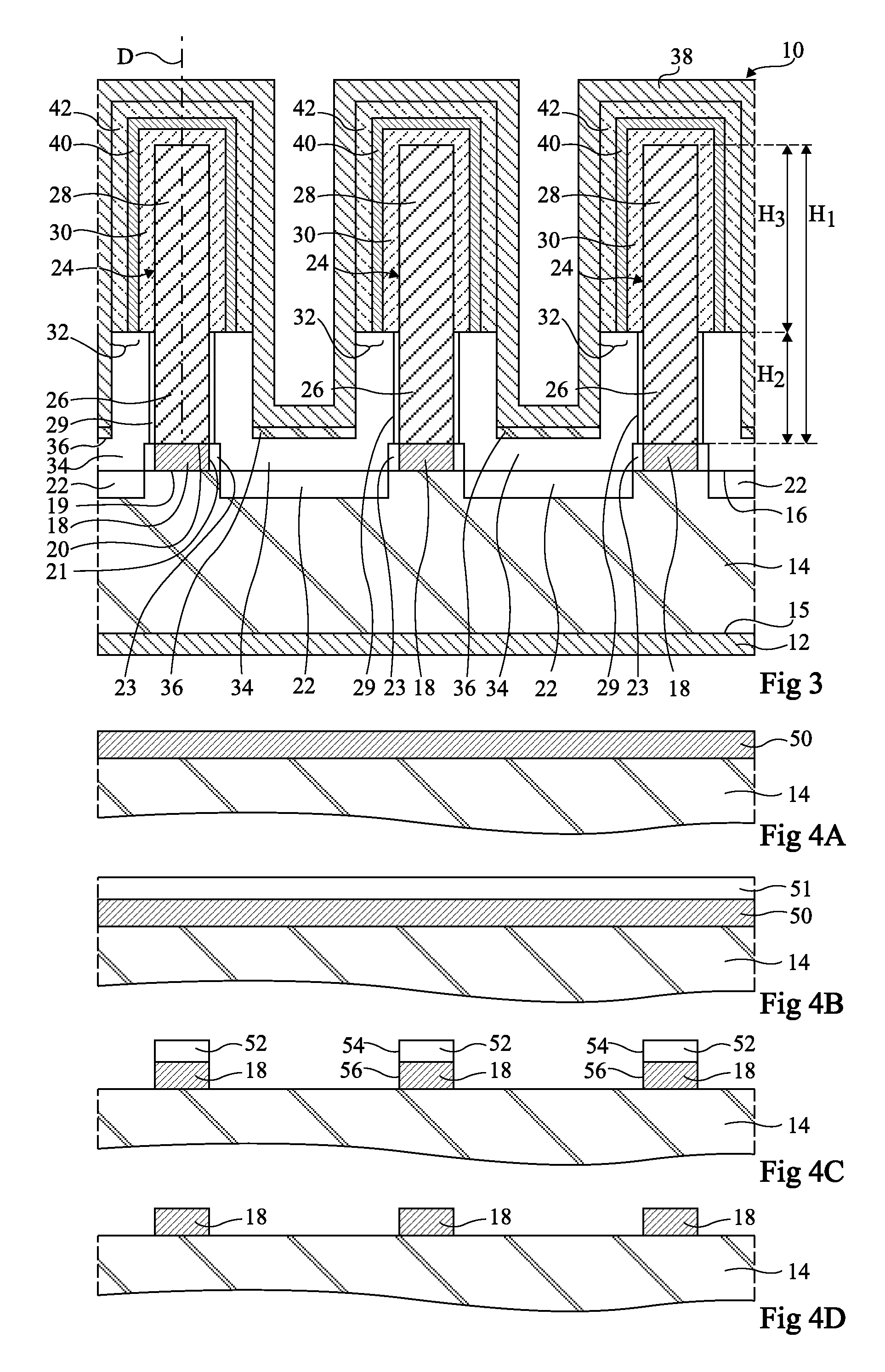
[0062]For clarity, the same elements have been designated with the same reference numerals in the various drawings and, further, as usual in the representation of electronic circuits, the various drawings are not to scale. Further, only those elements which are useful to the understanding of the present description have been shown and will be described. In particular, the optoelectronic device control means described hereafter are within the abilities of those skilled in the art and are not described.

[0063]In the following description, unless otherwise indicated, terms “substantially”, “approximately”, and “in the order of” mean “to within 10%”. Further, “compound mainly formed of a material” or “compound based on a material” means that a compound comprises a proportion greater than or equal to 95% of said material, this proportion being preferably greater than 99%.

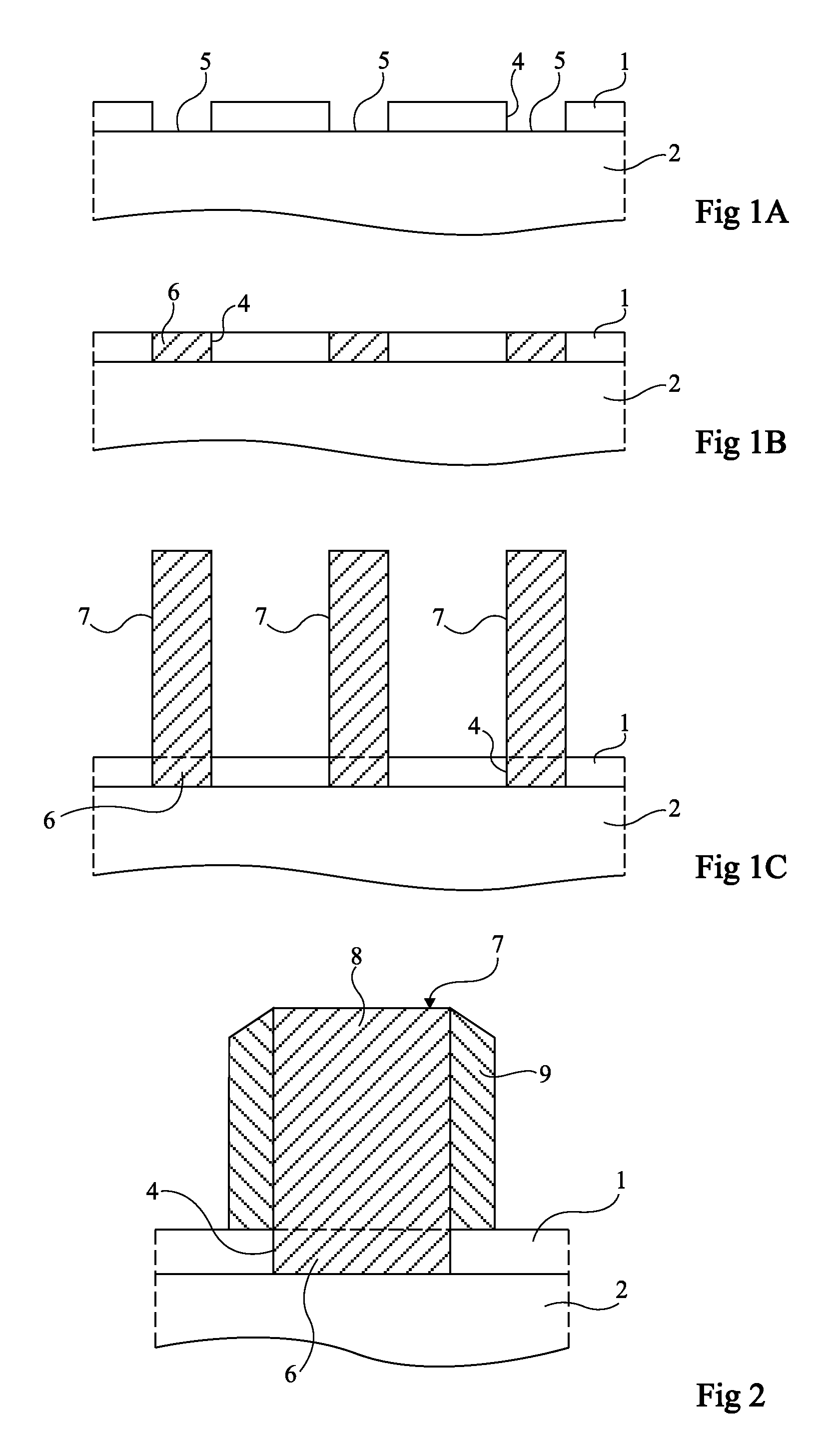
[0064]The present invention relates to the manufacturing of three-dimensional elements, for example, microwires, nanowi...


PUM


Abstract

An optoelectronic device comprises a substrate; pads on a surface of the substrate; semiconductor elements, each element resting on a pad; a portion covering at least the lateral sides of each pad, the portion preventing the growth of the semiconductor elements on the lateral sides; and a dielectric region extending in the substrate from the surface and connecting, for each pair of pads, one of the pads in the pair to the other pad in the pair. A method of manufacturing an optoelectronic device is also disclosed.

Description

CROSS REFERENCE TO RELATED APPLICATIONS[0001]The present patent application is the national stage application under 35 U.S.C. §371 of International Application No. PCT / FR2013 / 052551 filed Oct. 25, 2013 with priority claim to French patent application FR13 / 52794 and French patent application FR12 / 60232 the entire disclosures of which are incorporated herein by reference in their entireties.BACKGROUND[0002]The present invention generally relates to semiconductor materials, to devices based on semiconductor materials, and to their manufacturing methods. The present invention more specifically relates to devices comprising three-dimensional elements, and especially semiconductor microwires or nanowires.DISCUSSION OF THE RELATED ART[0003]Microwires or nanowires based on a compound mainly containing a group-III element and a group-V element (for example, gallium nitride GaN), called III-V compound hereafter, or mainly containing a group-II element and a group-VI element (for example, zinc...

Claims


Application Information

Patent Timeline
Patent Type & Authority Patents(United States)
IPC IPC(8): H01L21/20B82Y20/00H01L31/0224B82Y40/00H01L21/02H01L31/0352H01L33/00H01L33/08H01L33/18H01L31/18H01L33/38H01L33/24H01L31/0296H01L31/0304H01L31/028H01L21/36
CPCB82Y40/00H01L21/02458H01L21/0254H01L21/02603H01L21/0262H01L21/02639H01L31/035227H01L33/007H01L33/08H01L33/18H01L33/24H01L31/0296H01L31/0304H01L31/184H01L31/1828H01L31/1808H01L31/1804H01L31/035281H01L31/022408H01L33/38H01L33/0083H01L33/0062H01L33/0054H01L31/028H01L33/20H01L33/32H01L31/03044H01L31/03529B82Y20/00H01L21/02381H01L33/0075H01L33/0095H01L33/44H01L33/06H01L2933/0016H01L33/28H01L2933/0025Y02E10/544Y02E10/547Y02P70/50
Inventor DECHOUX, NATHALIEAMSTATT, BENO TGILET, PHILIPPE
Owner ALEDIA
Why Eureka
Try Eureka