Method for manufacturing light-emitting device

a technology of light-emitting devices and manufacturing methods, which is applied in the direction of semiconductor devices, organic semiconductor devices, electrical devices, etc., can solve the problems of burnt deposits, inability to form openings having a desired depth, damage to the bottom or periphery of openings,

Active Publication Date: 2016-05-03
SEMICON ENERGY LAB CO LTD
View PDF42 Cites 20 Cited by
  • Summary
  • Abstract
  • Description
  • Claims
  • Application Information

AI Technical Summary

Benefits of technology

[0011]The organic compound-containing layer is formed in an island shape in a region of the electrode terminal to which electric power from an external power supply and an external signal are input as well as over the first electrode layer. An interface between the organic compound-containing layer and the electrode terminal has low adhesion, and for this reason, the adhesive layer formed over the organic compound-containing layer over the electrode terminal can be easily separated from the electrode terminal. Thus, a cut is made in the organic layer to separate the organic layer, whereby the electrode terminal can be exposed.
[0012]When the method for manufacturing a light-emitting device of one embodiment of the present invention is employed, the organic layer can be removed to expose the electrode terminal in a shorter time than in the case of employing a laser ablation method, a dry etching method, an ion beam sputtering method, or the like. Moreover, the organic layer can be removed without damaging the electrode terminal.
[0015]When the method for manufacturing a light-emitting device of one embodiment of the present invention is employed, the second organic layer can be removed to expose the electrode terminal in a shorter time than in the case of employing a laser ablation method, a dry etching method, an ion beam sputtering method, or the like. Moreover, the second organic layer can be removed without damaging the electrode terminal.
[0019]According to one embodiment of the present invention, an opening through which an electrode terminal is exposed can be made in an organic resin or the like without damaging the electrode terminal. A flexible light-emitting device in which power and a signal can be input from the electrode terminal can be provided.

Problems solved by technology

However, in the case where an opening is formed in the organic film or the substrate by a laser ablation method or the like, the bottom or periphery of the opening might be damaged due to heat, or the opening having a desired depth might not be able to be formed.
Note that “damage due to heat” in this specification includes a burnt deposit, surface roughness, and the like.

Method used


Image

  • Method for manufacturing light-emitting device
  • Method for manufacturing light-emitting device
  • Method for manufacturing light-emitting device

Examples


embodiment 1

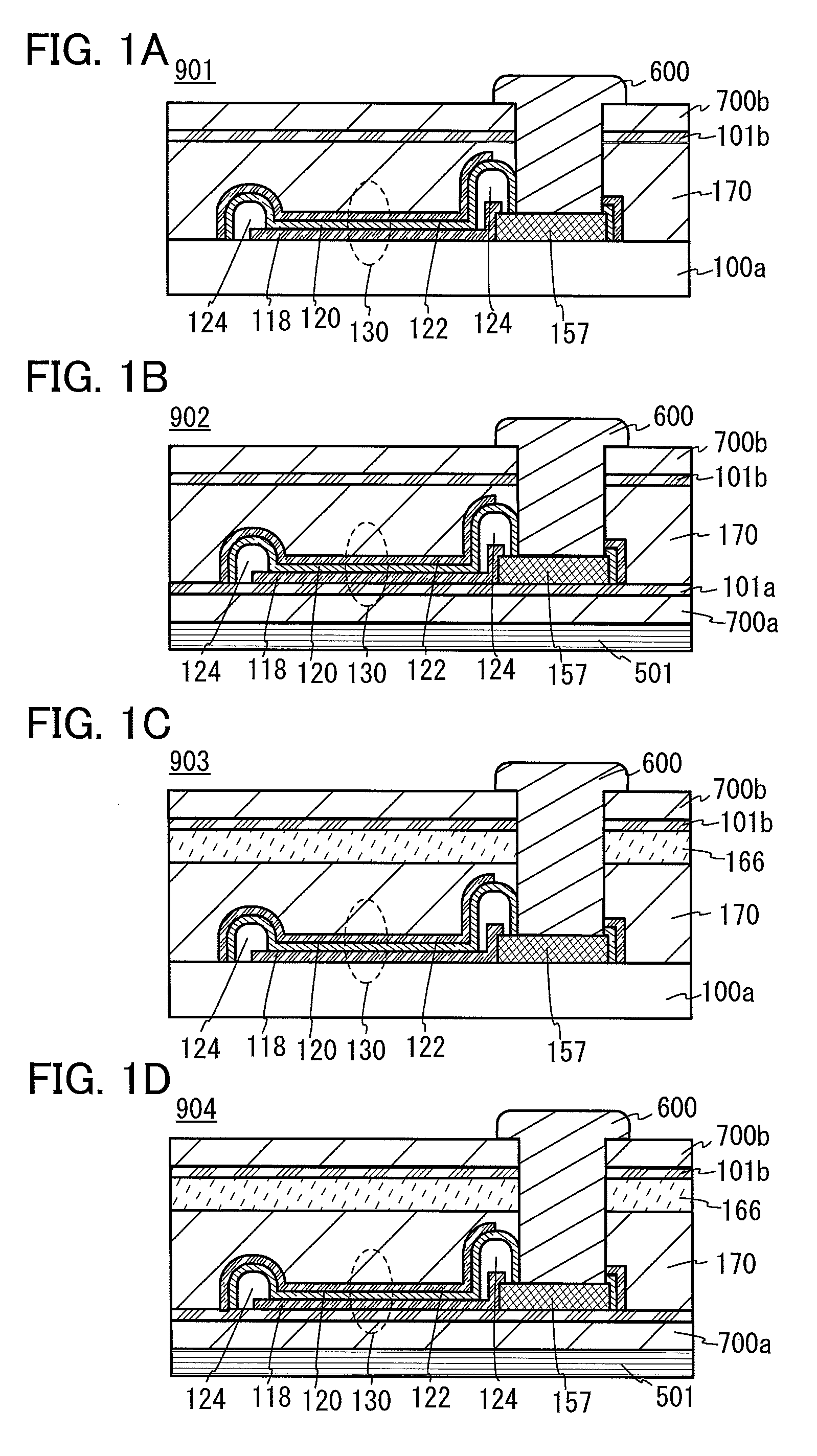
[0037]FIG. 1A is across-sectional view illustrating a light-emitting device 901 which can be manufactured by a method for manufacturing a light-emitting device of one embodiment of the present invention. The light-emitting device 901 includes an electrode terminal 157 and a first electrode layer 118 over a first substrate 100a. An edge portion of the first electrode layer 118 is covered with a partition wall 124 to be insulated. An organic compound-containing layer 120 is in contact with at least the top surfaces of the first electrode layer 118 and the partition wall 124. There is a part in which the organic compound-containing layer 120 does not exist over the electrode terminal 157. A second electrode layer 122 is in contact with at least a top surface of the organic compound-containing layer 120. The second electrode layer 122 does not exist over the electrode terminal 157. An adhesive layer 170 is in contact with the second electrode layer 122. The adhesive layer 170 does not e...

modification example 1

of Method for Manufacturing Light-Emitting Device

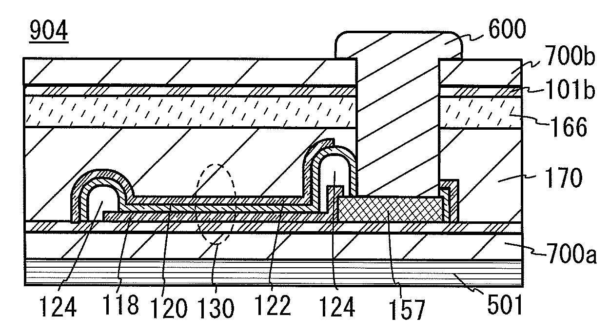
[0071]FIG. 1B is a cross-sectional view of a light-emitting device 902 which can be manufactured by a method for manufacturing a light-emitting device of one embodiment of the present invention. The light-emitting device 902 includes a flexible substrate 501 and the second organic layer 700b, and is thus flexible. The method for manufacturing the light-emitting device 902 is different from the method for manufacturing the light-emitting device 901 in that the first separation layer 101a is formed between the first substrate 100a and the light-emitting element 130.

[0072]In this modification example, in the case of using a glass substrate as the first substrate 100a, an insulating layer such as a silicon oxide film, a silicon oxynitride film, a silicon nitride film, or a silicon nitride oxide film is preferably formed between the first substrate 100a and the first separation layer 101a, in which case contamination due to an alkali metal...

modification example 2

of Method for Manufacturing Light-Emitting Device

[0087]FIG. 1C is a cross-sectional view of a light-emitting device 903 which can be manufactured by a method for manufacturing a light-emitting device of one embodiment of the present invention. In the light-emitting device 903, a coloring layer 166 is provided between the adhesive layer 170 and the second separation layer 101b. The other structures are the same as those of the light-emitting device 901; thus, the above embodiment can be referred to for the other structures. Therefore, only a method for forming the coloring layer 166 will be described below.

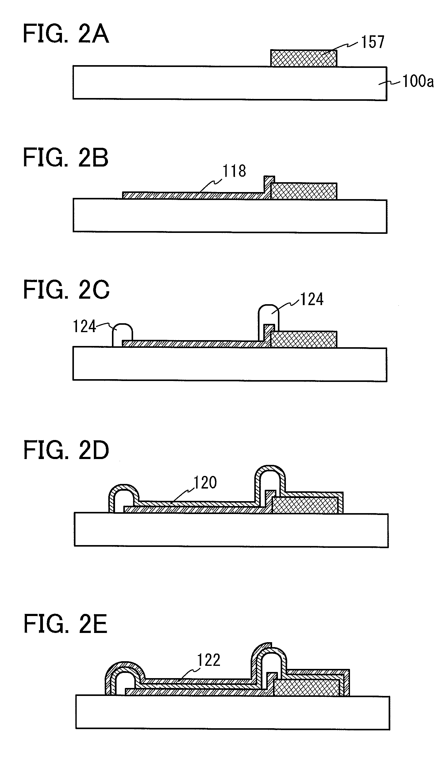
[0088]The formation steps of the light-emitting device 901 (FIGS. 2A to 2E) can be referred to for the steps up to and including the formation of the second electrode layer 122.

(Coloring Layer)

[0089]The coloring layer 166 is formed on the second separation layer 101b on the second substrate 100b. Note that in FIG. 6C, the second separation layer 101b and the coloring layer 166 are ...


PUM


Abstract

A method for exposing an electrode terminal covered with an organic film in a light-emitting device without damaging the electrode terminal is provided. In a region of the electrode terminal to which electric power from an external power supply or an external signal is input, an island-shaped organic compound-containing layer is formed and the organic film is formed thereover. The organic film is removed by utilizing low adhesion of an interface between the organic compound-containing layer and the electrode terminal, whereby the electrode terminal can be exposed without damage to the electrode terminal.

Description

BACKGROUND OF THE INVENTION[0001]1. Field of the Invention[0002]The present invention relates to a method for manufacturing a light-emitting device.[0003]2. Description of the Related Art[0004]In recent years, research and development have been extensively conducted on light-emitting elements using electroluminescence (EL). In a basic structure of such a light-emitting element, a layer containing a substance with a light-emitting property is interposed between a pair of electrodes. By voltage application to this element, light emission can be obtained from the light-emitting substance.[0005]The above light-emitting element is a self-luminous element; thus, a light-emitting device using the light-emitting element has advantages such as high visibility, no necessity of a backlight, and low power consumption. The light-emitting device using the light-emitting element also has advantages in that it can be manufactured to be thin and lightweight and has fast response speed.[0006]Since a ...

Claims


Application Information

Patent Timeline
Patent Type & Authority Patents(United States)
IPC IPC(8): H01L51/56H01L27/12H01L51/52H01L27/32
CPCH01L51/56H01L27/1225H01L27/3276H01L27/3246H01L51/5237H01L2227/323H01L2227/326H01L2251/5338H10K59/122H10K59/131H10K50/844H10K50/8426H10K71/80H10K59/1201H10K71/00H10K2102/311H05K2201/05H10K59/123H10K50/80H10K50/84H10K50/805
Inventor CHIDA, AKIHIROHATANO, KAORUAOYAMA, TOMOYAKOMATSU, RYUKATANIWA, MASATOSHI
Owner SEMICON ENERGY LAB CO LTD
Why Eureka
Try Eureka