Method for manufacturing semiconductor device

a semiconductor and manufacturing technology, applied in the direction of sustainable manufacturing/processing, final product manufacturing, instruments, etc., can solve the problems of difficult to finely control the temperature of all treatment steps during the manufacturing process, plastic film may contaminate an element, plastic film has less heat resistance, etc., and achieves the effect of smooth peeling step

Active Publication Date: 2007-11-01
SEMICON ENERGY LAB CO LTD
View PDF50 Cites 83 Cited by
  • Summary
  • Abstract
  • Description
  • Claims
  • Application Information

AI Technical Summary

Benefits of technology

[0034]According to the present invention, a peeling step can be carried out smoothly even in a case of using a large substrate with a diagonal length of more than 1 m.

Problems solved by technology

Further, a plastic film may contaminate an element by absorbing or releasing moisture or the like during the process of manufacturing a TFT.
Furthermore, a plastic film has lower heat resistance and is more significantly expanded and contracted due to heat as compared to a glass substrate, but it is difficult to finely control all treatment temperatures during the manufacturing process.
Molybdenum has the disadvantage of being inferior in heat resistance to tungsten.
For example, a molybdenum film causes peeling when subjected to heat treatment at 500° C. or higher; therefore, the temperature during the manufacturing process is preferably lower than 500° C. Further, a molybdenum film formed by a sputtering method is fragile, and is particularly fragile at the crystal grain boundary in a polycrystalline state.

Method used


Image

  • Method for manufacturing semiconductor device
  • Method for manufacturing semiconductor device
  • Method for manufacturing semiconductor device

Examples


embodiment mode 1

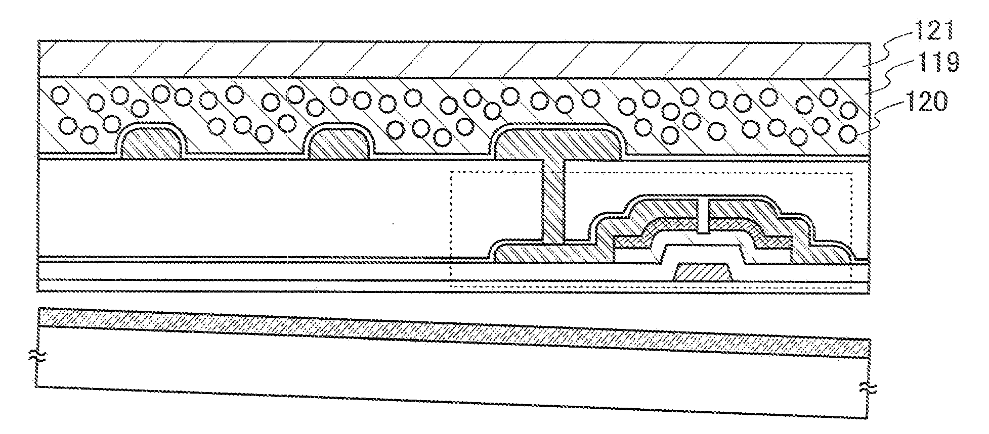
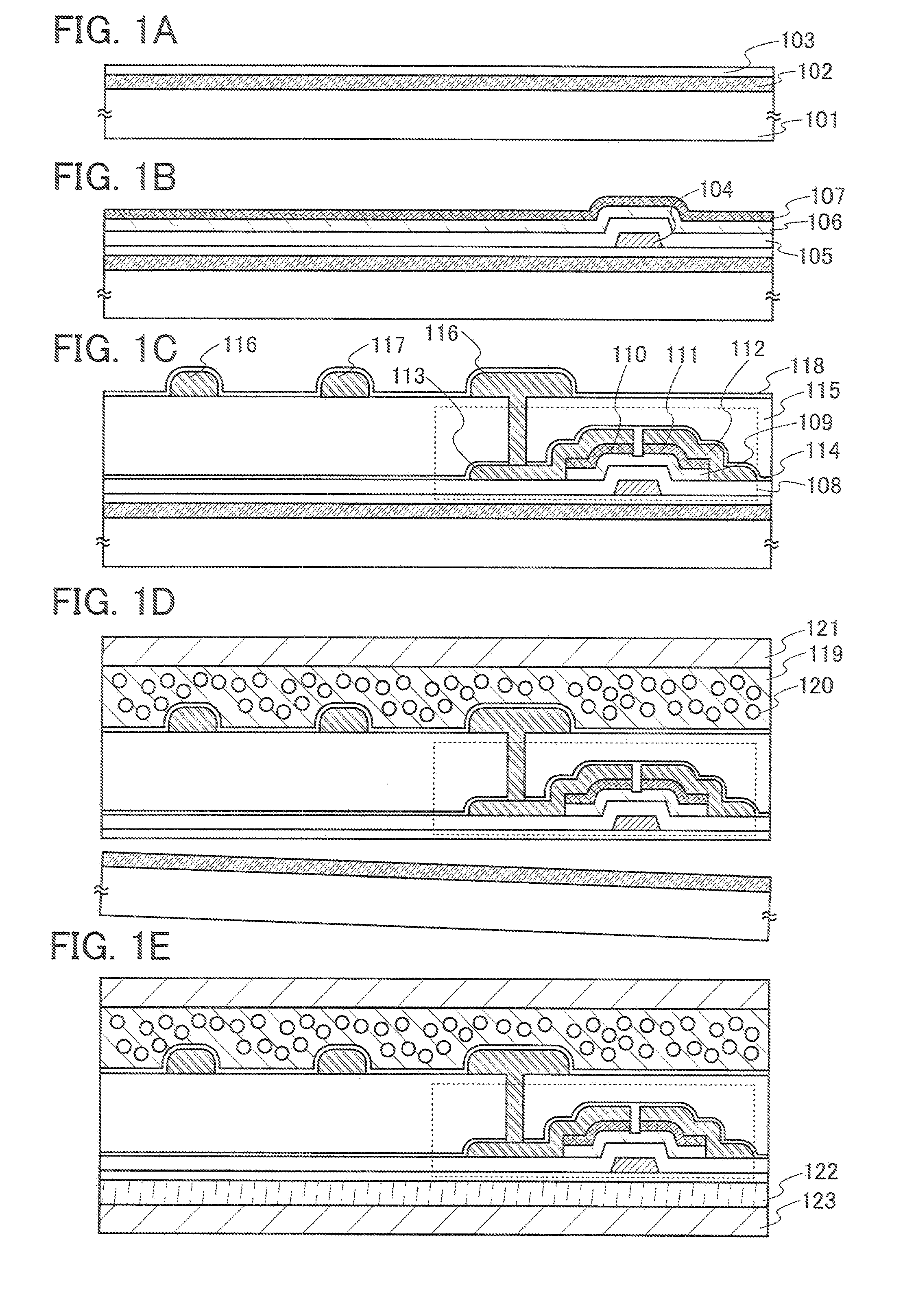
[0052]An example of manufacturing a liquid crystal display device is explained here with reference to FIGS. 1A to 1E.

[0053]First, a molybdenum film 102 is formed over a substrate 101. The substrate 101 used here is a glass substrate. The molybdenum film 102 is a molybdenum film formed by a sputtering method with a thickness of 30 nm to 200 nm. Since the substrate may be fixed for a sputtering method, the thickness of the molybdenum film on the edge portion of the substrate tends to be nonuniform. Therefore, the molybdenum film on the edge portion is preferably removed by dry etching.

[0054]Next, a molybdenum oxide film 103 is formed by oxidation of a surface of the molybdenum film 102. The molybdenum oxide film 103 may be formed by oxidation of the surface with the use of pure water or ozone water or with the use of oxygen plasma. Alternatively, the molybdenum oxide film 103 may be formed by heating in an atmosphere including oxygen. FIG. 1A shows a cross-sectional view at a stage wh...

embodiment mode 2

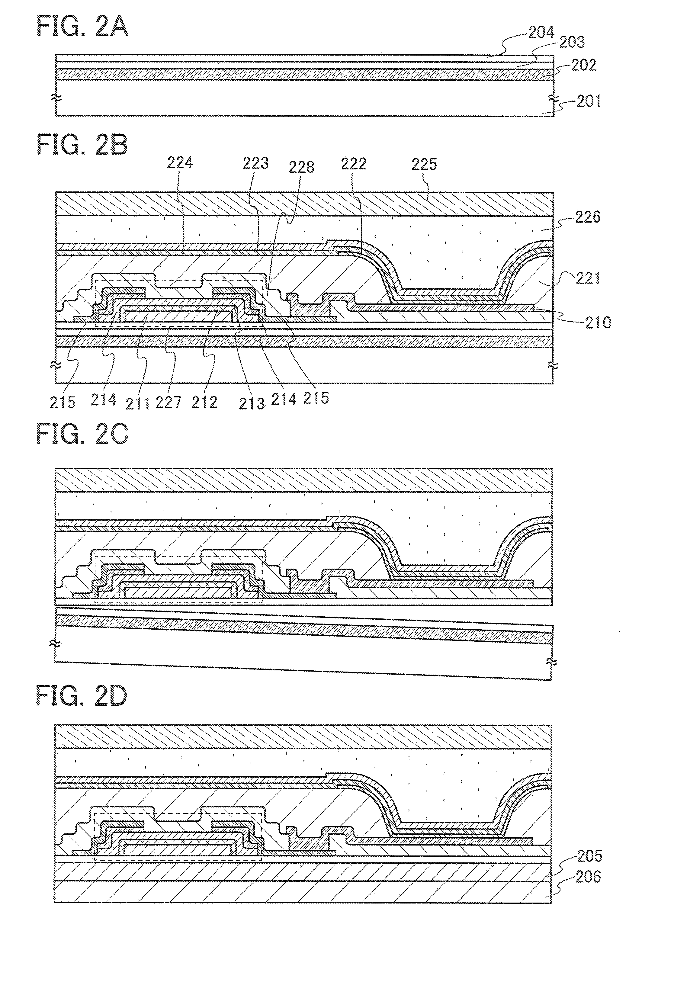
[0073]Described here with reference to FIGS. 2A to 2D is an example of manufacturing an active-matrix light emitting device using an organic TFT.

[0074]First, a molybdenum film 202 is formed over a substrate 201. The substrate 201 used here is a glass substrate. The molybdenum film 202 is a molybdenum film formed by a sputtering method with a thickness of 30 nm to 200 nm.

[0075]Next, a molybdenum oxide film 203 is formed by oxidation of a surface of the molybdenum film 202. The molybdenum oxide film 203 may be formed by oxidation of the surface with the use of pure water or ozone water or with the use of oxygen plasma. Alternatively, the molybdenum oxide film 203 may be formed by heating in an atmosphere including oxygen. Further alternatively, it may be formed in a later step of forming an insulating film. When a silicon oxide film or a silicon oxynitride film is formed as the insulating film by a plasma CVD method, the surface of the molybdenum film 202 is oxidized; accordingly, the...

embodiment mode 3

[0103]An example of manufacturing a passive-matrix light emitting device over a flexible substrate is described here with reference to FIGS. 5A to 9.

[0104]In a passive (simple-matrix) light emitting device, a plurality of anodes arranged in stripes (strip-form) are provided perpendicularly to a plurality of cathodes arranged in stripes. A light emitting layer or a fluorescent layer is interposed at each intersection. Therefore, a pixel at an intersection of an anode selected (to which a voltage is applied) and a cathode selected emits light.

[0105]FIG. 5A shows a top view of a pixel portion before sealing. FIG. 5B shows a cross-sectional view taken along a dashed line A-A′ in FIG. 5A. FIG. 5C shows a cross-sectional view taken along a dashed line B-B′.

[0106]A molybdenum film 502, a molybdenum oxide film 503, and an insulating film 504 are stacked over a first substrate 501 similarly to Embodiment Mode 2. A plurality of first electrodes 513 are arranged in stripes at regular intervals...


PUM

PropertyMeasurementUnit
thicknessaaaaaaaaaa
temperatureaaaaaaaaaa
thicknessaaaaaaaaaa

Abstract

A technique for peeling an element manufactured through a process at relatively low temperature (lower than 500° C.) from a substrate and transferring the element to a flexible substrate (typically, a plastic film). With the use of an existing manufacturing device for a large glass substrate, a molybdenum film (Mo film) is formed over a glass substrate, an oxide film is formed over the molybdenum film, and an element is formed over the oxide film through a process at relatively low temperature (lower than 500° C.). Then, the element is peeled from the glass substrate and transferred to a flexible substrate.

Description

BACKGROUND OF THE INVENTION[0001]1. Field of the Invention[0002]The present invention relates to a semiconductor device which has a circuit including a thin film transistor (hereinafter referred to as a TFT) and a method for manufacturing the semiconductor device. For example, the present invention relates to an electronic device which has as a component an electro-optical device typified by a liquid crystal display panel or a light emitting display device including an organic light emitting element.[0003]Note that the term “semiconductor device” in this specification refers to a device in general that can operate by utilizing semiconductor characteristics, and an electro-optical device, a semiconductor circuit, and an electronic device are all included in the semiconductor device.[0004]2. Description of the Related Art[0005]In recent years, attention has been focused on a technique for forming a thin film transistor (TFT) with the use of a semiconductor thin film (with a thickness ...

Claims


Application Information

Patent Timeline
Patent Type & Authority Applications(United States)
IPC IPC(8): H01L21/30G02F1/167
CPCG02F1/167G02F2001/13613H01L2924/0002G06K19/07749H01L21/7806H01L23/49855H01L23/645H01L23/66H01L27/1214H01L27/1266H01L51/003H01L51/0097H01L2223/6677H01L2924/09701H01L2924/12044H01L2924/3011Y02E10/549H01L2924/00H01L27/1218Y02P70/50G02F1/13613H10K71/80H10K77/111H10K59/1201H01L27/1225H01L29/78603H01L29/7869
Inventor MARUYAMA, JUNYAJINBO, YASUHIROSHOJI, HIRONOBU
Owner SEMICON ENERGY LAB CO LTD
Why Eureka
Try Eureka