

Method for treatment of a temporarily bonded product wafer
a technology of product wafers and adhesives, which is applied in the direction of decorative surface effects, chemical vapor deposition coatings, decorative arts, etc., can solve the problems of serious problems such as the phenomenon of dimples, problems such as the further processing of problems, and achieve the effect of easy flow of adhesives, low intrinsic stiffness of product wafers, and high adhesive thickness
Active Publication Date: 2016-06-07
EV GRP E THALLNER GMBH
View PDF21 Cites 0 Cited by
- Summary
- Abstract
- Description
- Claims
- Application Information
AI Technical Summary
Benefits of technology
The text discusses how the problem of dimples (small bumps) on semiconductor wafers has become more serious in recent times. This is because thin wafers are now being preferred, which means the stiffness of the wafer decreases as it gets thinner. This decrease in stiffness leads to less stable wafers and makes it difficult to counteract the stress that arises due to crystal defects. However, if there are no surface defects, the quality of the wafer is improved significantly. Therefore, the technical effect of this patent text is to provide a solution to improve the quality of semiconductor wafers by reducing or eliminating surface defects such as dimples.
Problems solved by technology
If the surface defects were not avoided, problems would arise in the further processing.
The phenomenon of dimples has become a serious problem only in the recent past.
Especially unfavorable conditions in conjunction with dimple formation arise when, as the thickness of the wafers decreases, they also have increasing topography on the front and are to be embedded in the adhesive located between the carrier and product wafer.
Method used
View moreImage
Smart ImageViewing Examples

Examples
Embodiment Construction
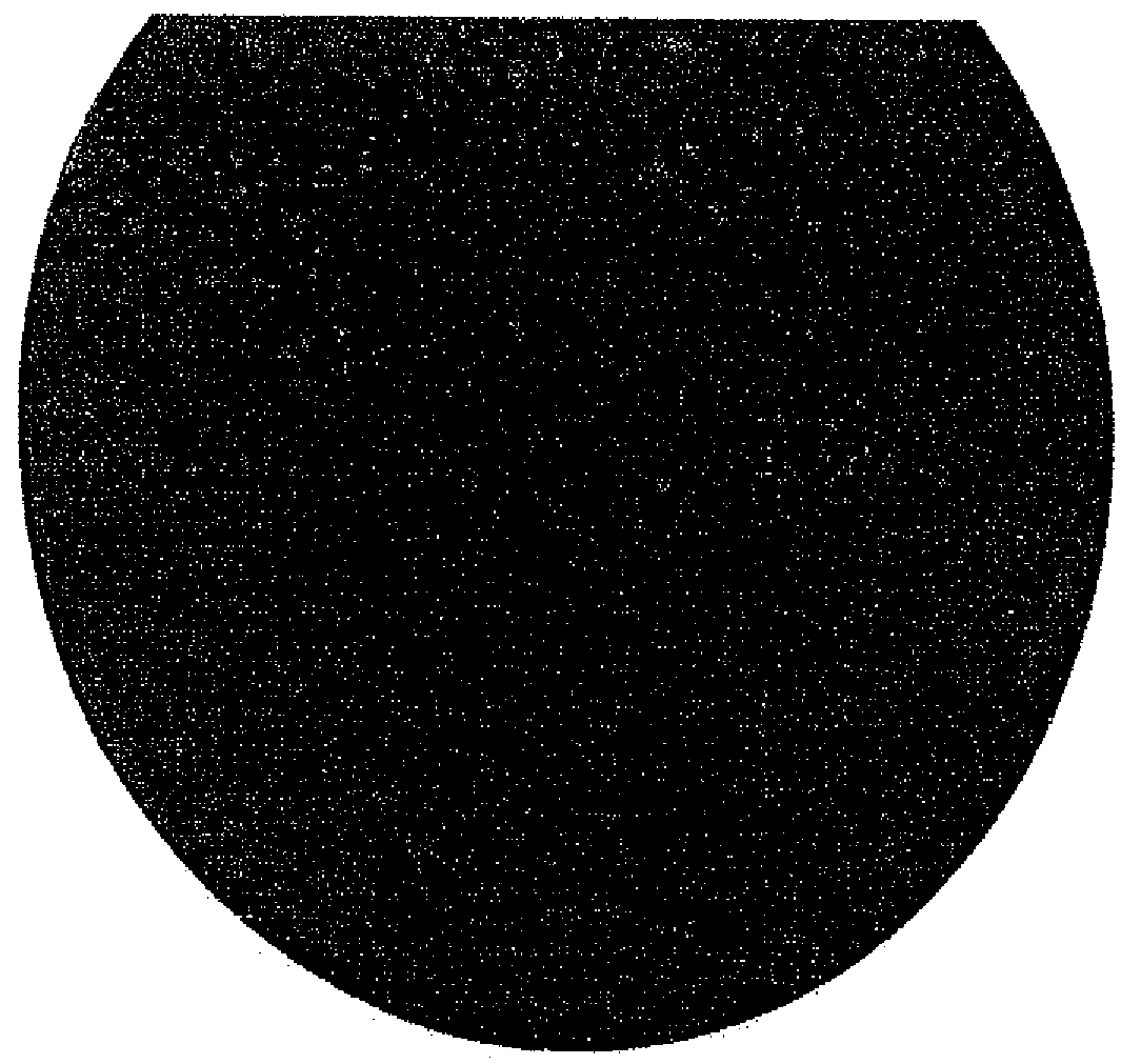
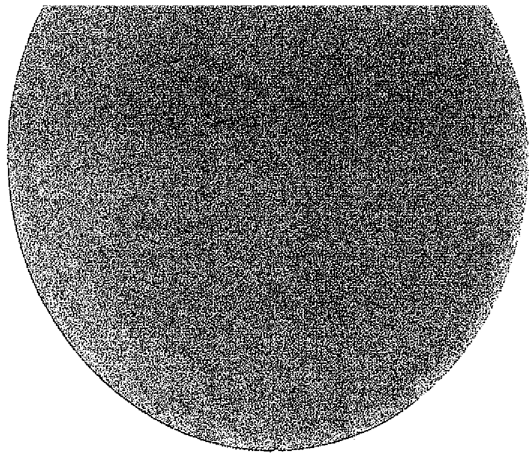
[0044]The figures show that the product wafer as shown in FIG. 1 has distinct dimples, whereas the product wafer shown in FIG. 2 has practically no dimples.
Login to View More PUM
| Property | Measurement | Unit |
|---|---|---|
| thickness | aaaaa | aaaaa |
| thickness | aaaaa | aaaaa |
| temperature | aaaaa | aaaaa |
Abstract
A method for treatment of a product wafer temporarily bonded on a carrier wafer with the following steps: grinding and / or backthinning of the product wafer on one flat side facing away from the carrier wafer to a product wafer thickness D of <150 μm, especially <100 μm, preferably <75 μm, even more preferably <50 μm, especially preferably <30 μm, surface treatment of the flat side with means for reducing an especially structural intrinsic stress of the product wafer.
Description
FIELD of INVENTION[0001]The invention relates to a method and a device for treatment of a temporarily bonded wafer.BACKGROUND of INVENTION[0002]Novel, three-dimensional integrated circuits require reliable methods for handling of thin wafers in order to be able to successfully transport the thin wafers through the necessary product processes on the wafer back. The method of temporary bonding had become established in past years. In it the product wafer with a fully or partially finished first main surface is mounted on a carrier by means of a suitable method, especially by means of adhesive technology. Here this first main surface points in the direction of the carrier wafer. The product wafer is then thinned by means of known grinding techniques. After this thinning process other production steps are carried out on the back of the thin wafer. In the past, processes in which high thermal stresses were produced in the wafer, such as for example abrupt heating and / or cooling, led to p...
Claims
Login to View More Application Information
Patent Timeline
 Patent Type & AuthorityPatents(United States)
IPC IPC(8): H01L21/304H01L21/683
CPCH01L21/6835H01L21/6836H01L2221/6834H01L2221/68327H01L21/304H01L21/683
InventorBURGGRAF, JURGENWIESBAUER, HARALDWIMPLINGER, MARKUS
OwnerEV GRP E THALLNER GMBH