Touch panel and a manufacturing method thereof
a technology of touch panel and manufacturing method, which is applied in the field of touch panel, can solve the problems that the conventional design of the touch panel cannot meet the requirements, and achieve the effect of reducing the peripheral area, increasing the available touch area, and reducing the area of the peripheral area
- Summary
- Abstract
- Description
- Claims
- Application Information
AI Technical Summary
Benefits of technology
Problems solved by technology
Method used
Image
Examples
first embodiment
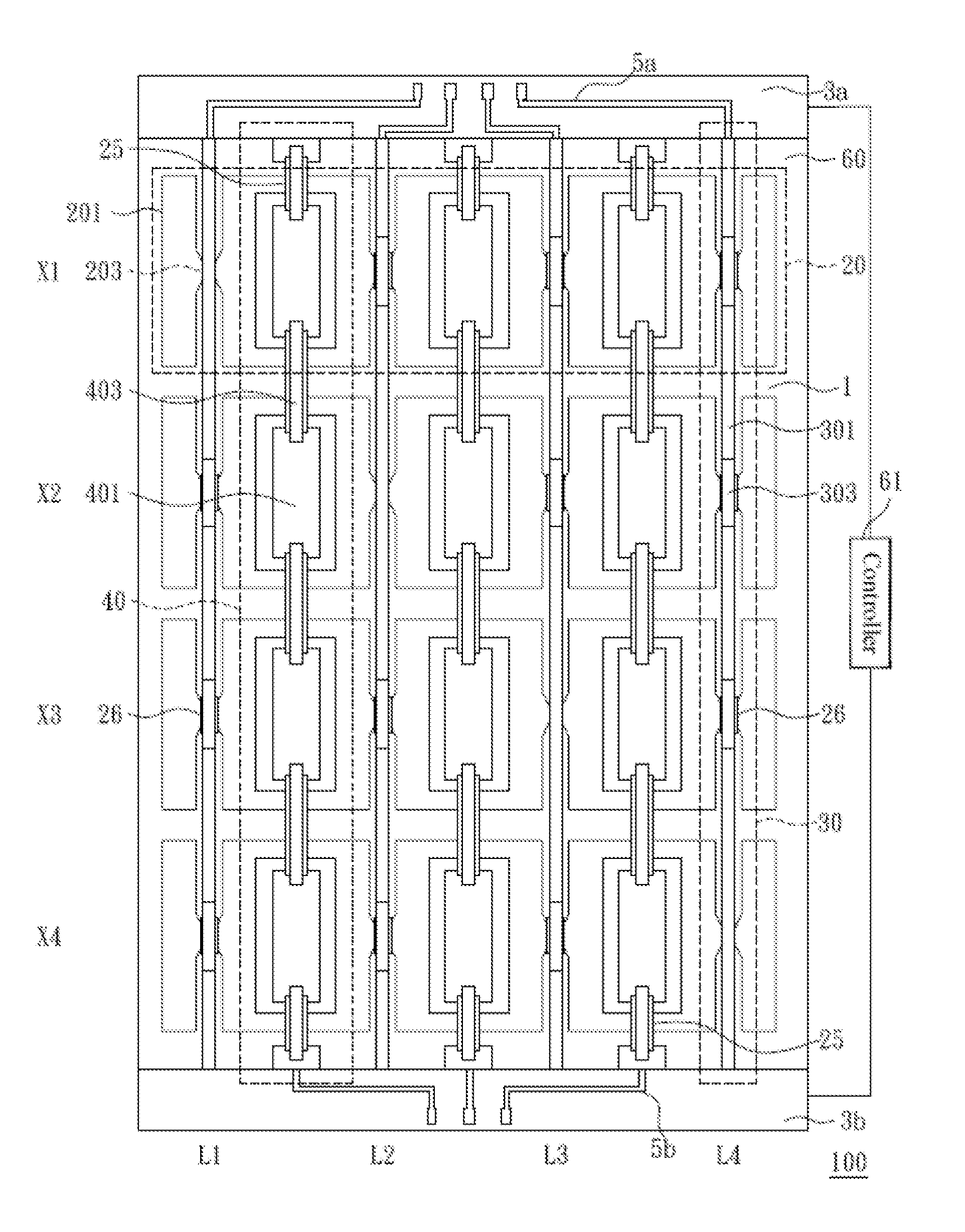
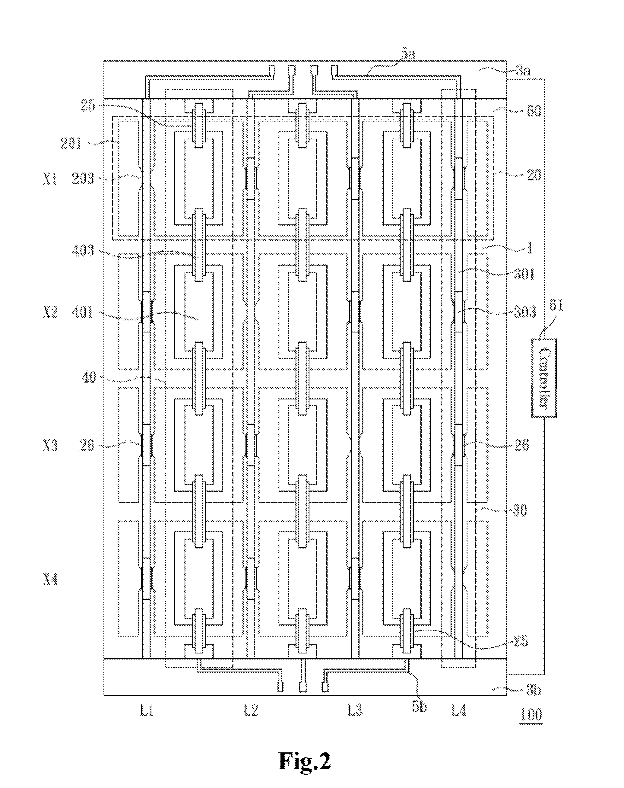
[0022]FIG. 2 is a schematic structure view of a touch panel in accordance with the present disclosure. A touch panel 100 has a touch area 1 and a first peripheral area 3a. The touch panel 100 comprises a plurality of first sensing electrode axes 20, a plurality of second sensing electrode axes 40, and a plurality of conductive wire axes 30. The first sensing electrode axes 20 and the second sensing electrode axes 40 are disposed on the touch area 1 along a first axis and a second axis respectively. The first sensing electrode axes 20 are electrically insulated from the second sensing electrode axes 40. The conductive wire axes 30 are disposed on the touch area 1 along the second axis and are extended to the first peripheral area 3a, wherein any two of the conductive wire axes 30 are electrically connected to different first sensing electrode axes 20, and wherein the first peripheral area 3a is located at a first side of the touch area 1.
[0023]Specifically, in the present embodiment,...
second embodiment
[0052]FIGS. 11˜12 are schematic views illustrating a method for manufacturing a touch panel in accordance with the present disclosure. The manufacturing method in the present embodiment is used to form the touch panel 100 shown in FIG. 3 correspondingly.
[0053]First manufacturing process of the present embodiment is approximately identical to the first manufacturing process of the first embodiment, as shown in FIG. 6. For conciseness, no more description is made herein.
[0054]In a second manufacturing process, as shown in FIG. 11, a plurality of first insulation blocks 25 and a plurality of second insulation blocks 26 are formed, wherein each of the first insulation blocks 25 is disposed on the first electrodes 201 between the adjacent second electrodes 401 and each of the second insulation blocks 26 is disposed on the first conductive wire 203 at an insulation point such that conductive wire axes 30 and first sensing electrode axes 20 to be formed subsequently are electrically connec...
third embodiment
[0057]FIGS. 13˜14 are schematic views illustrating a method for manufacturing a touch panel in accordance with the present disclosure. The manufacturing method in the present embodiment is used to form the touch panel 100 shown in FIG. 4 correspondingly.
[0058]First and second manufacturing processes of the present embodiment are approximately identical to the first and second manufacturing processes of the first embodiment, as shown in FIG. 6 and FIG. 7. Thus, no more description is made herein.
[0059]Difference between the present embodiment and the first embodiment at least lies in that: as shown in FIG. 13, in a third manufacturing process, an insulation layer 77 is formed on the first electrodes 201, the first conductive wires 203, the second electrodes 401, and the conductive wire segments 301. There are a plurality of first through-holes 771 and a plurality of second through-holes 772 on the surface of the insulation layer 77, wherein the first through-holes 771 correspond to t...
PUM
| Property | Measurement | Unit |
|---|---|---|
| area | aaaaa | aaaaa |
| conductive | aaaaa | aaaaa |
| size | aaaaa | aaaaa |
Abstract
Description
Claims
Application Information


