

Method of manufacturing alignment film
a technology of alignment film and alignment film, which is applied in the direction of electrical equipment, semiconductor devices, instruments, etc., can solve the problems of light leakage, unevenness of image display, etc., and achieve the effect of less mura and better quality
- Summary
- Abstract
- Description
- Claims
- Application Information
AI Technical Summary
Benefits of technology
Problems solved by technology
Method used
Image

Examples
embodiment 1
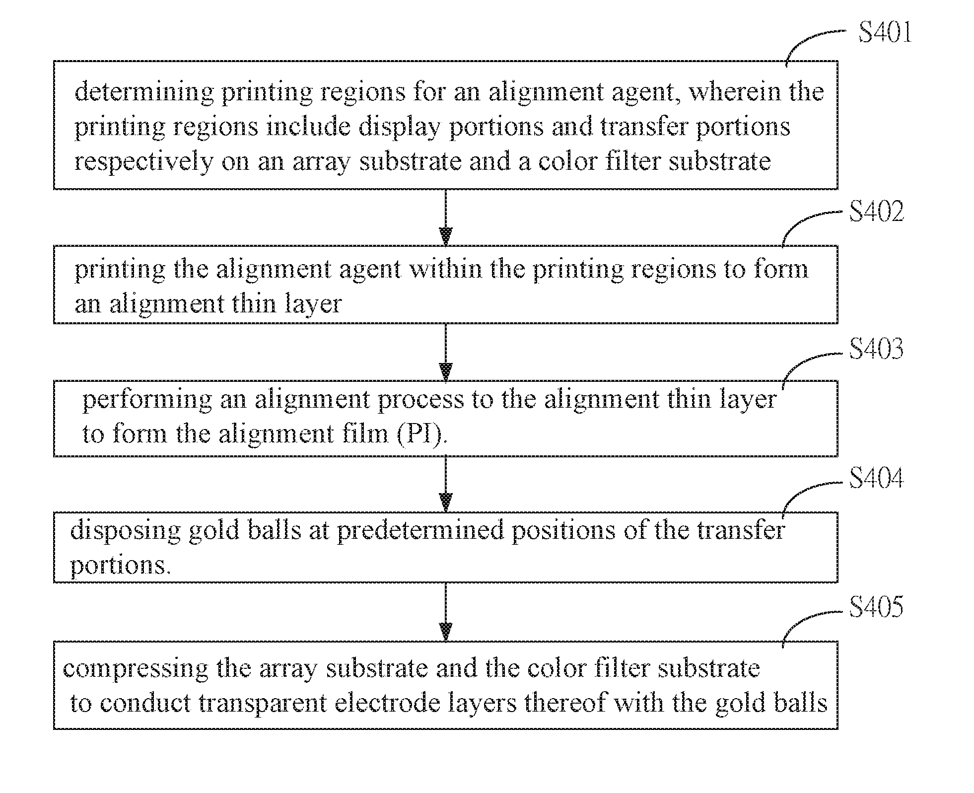
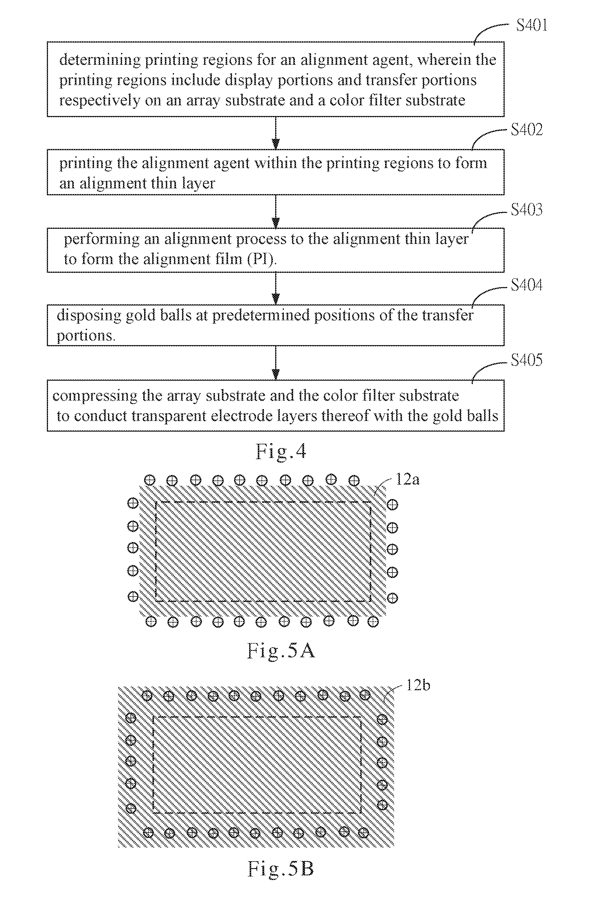
[0029]Please refer to FIG. 4, a method of manufacturing an alignment film according to one embodiment of the present invention for providing an alignment film having an even thickness and a clear edge of display is illustrated, and comprises the following steps.
[0030]In step S401, printing regions respectively on an array substrate and a color filter substrate are determined first, wherein the printing regions include display portions and transfer portions.
[0031]Conceivably, the display portions on the array substrate and the color filter substrate are used for displaying images after forming a liquid crystal panel, as shown by 12a in FIG. 5A.
[0032]Conceivably, the transfer portions surround the display portions, and a sealant is applied thereon for connecting the array substrate and the color filter substrate. In general, where a transparent electrode layer is disposed corresponds to the transfer portions on the array substrate or the color filter substrate, and electric gold balls...
embodiment 2
[0042]The present invention provides a method of manufacturing an alignment film for providing an alignment film having an even thickness and a clear edge of display. The method is based on the first embodiment, and has additional steps of cleaning the transfer portions between step S402 and S403. The additional steps comprise (1) applying a stripping agent within the transfer portions, wherein the stripping agent is used for dissolving the alignment thin layer covering on the transfer portions; and (2) cleaning the transfer portions for removing the stripping agent and impurities after dissolving the alignment thin layer. Thus, the uniformity of the alignment film is improved; meanwhile, the connection status between the upper and lower substrates through the gold balls can be improved. The cross-sectional structure is as shown in FIG. 7.
[0043]Referring now to FIG. 7, the array substrate and the color filter substrate 11 have the transfer portions 13 thereon. The alignment film 12′...
embodiment 3
[0046]The present invention provides a method of manufacturing an alignment film for providing an alignment film having an even thickness and a clear edge of display. The method is based on the first embodiment, and has additional steps of (1) forming a transparent electrode layer having a ring shape on the transfer portion surrounding the display portion for improving the conductivity of the upper and lower substrates through the gold balls when preparing the array substrate, wherein the transparent electrode layer having a ring shape is shown as 11a in FIG. 8; and (2) mixing the sealant with the gold balls and applying on the transparent electrode layer having a ring shape. In step (2), the gold balls uniformly disperse in the sealant so that the chance of passing through the alignment film can be greatly raised, and the conductivity of the upper and lower substrate can be improved. The cross-sectional structure is as shown in FIG. 9.
[0047]In FIG. 9, transparent electrode layers (...
PUM
| Property | Measurement | Unit |
|---|---|---|
| thickness | aaaaa | aaaaa |
| transparent | aaaaa | aaaaa |
| power | aaaaa | aaaaa |
Abstract
Description
Claims
Application Information