Nanostructure-based transparent conductors having increased haze and devices comprising the same

a transparent conductor and nanostructure technology, applied in the direction of conductors, conductive layers on insulating supports, semiconductor devices, etc., can solve the problems of limited application, low light transmission and high haze, and high light scattering, etc., to achieve increased haze/light scattering, good device performance, and different and tunable scattering degrees

Active Publication Date: 2017-03-07
CHAMP GREAT INTL
View PDF36 Cites 3 Cited by
  • Summary
  • Abstract
  • Description
  • Claims
  • Application Information

AI Technical Summary

Benefits of technology

[0009]The present disclosure relates to modifications to nanostructure-based transparent conductors to achieve increased haze / light-scattering with different and tunable degrees of scattering. These modified transparent conductors are suitable for any device that employs transparent electrodes. They are particularly suited as front and / or back electrodes in opto-electrical device that is capable of converting light to electricity (e.g., PV) or electricity to light (e.g., light-emitting diode or organic light-emitting diode). In addition to the macroscopically measured haze value, the microscopic structure of hazy / scattering layer may be important for good device performance, including, e.g., enhancing contact and work function.
[0010]Various embodiments described a variety of light-scattering materials or media that can be combined with nanostructure-based transparent conductors in a variety of configurations. The scattering media may be of diverse materials as well as morphologies (including microstructures and nanostructures), thus allowing customization and tuning of the light-scattering to meet the performance parameters of the device incorporating the transparent conductor.

Problems solved by technology

However, this approach is limited by the nature of the TCOs (e.g., their chemical and physical micro-structure) in the types of scattering structure that can be achieved.
As a general rule for nanostructure-based transparent conductors, lower sheet resistance is typically associated with more conductive nanostructures, which in turn results in lower light transmission and higher haze.
Although this level of light-scattering is typically too high for displays, touch-panel and certain other applications, it may be too low for thin film PV applications.

Method used


Image

  • Nanostructure-based transparent conductors having increased haze and devices comprising the same
  • Nanostructure-based transparent conductors having increased haze and devices comprising the same
  • Nanostructure-based transparent conductors having increased haze and devices comprising the same

Examples


example 1

Synthesis of Silver Nanowires

[0088]Silver nanowires were synthesized by the reduction of silver nitrate dissolved in ethylene glycol in the presence of poly(vinyl pyrrolidone) (PVP) following the “polyol” method described in, e.g., Y. Sun, B. Gates, B. Mayers, & Y. Xia, “Crystalline silver nanowires by soft solution processing,”Nanoletters 2(2): 165-168, 2002. A modified polyol method, described in co-pending and co-owned U.S. patent application Ser. No. 11 / 766,552, produces more uniform silver nanowires at higher yields than does the conventional “polyol” method. This application is incorporated by reference herein in its entirety. Resulting nanowires primarily had lengths from about 13 μm to about 17 μm and diameters from about 34 nm to about 44 nm.

example 2

Standard Preparation of Ink Composition of Conductive Nanostructures

[0089]A typical ink composition for depositing metal nanowires comprises, by weight, from 0.0025% to 0.1% surfactant (e.g., a preferred range is from 0.0025% to 0.05% for ZONYL® FSO-100), from 0.02% to 4% viscosity modifier (e.g., a preferred range is 0.02% to 0.5% for hydroxypropyl methylcellulose (HPMC), from 94.5% to 99.0% solvent and from 0.05% to 1.4% metal nanowires. Representative examples of suitable surfactants include ZONYL® FSN, ZONYL® FSO, ZONYL® FSA, ZONYL® FSH, Triton (x100, x114, x45), TERGITOL®, DYNOL® (604, 607), n-dodecyl β-D-maltoside, and NOVEC®. Examples of suitable viscosity modifiers include hydroxypropyl methyl cellulose (HPMC), methyl cellulose, xanthan gum, polyvinyl alcohol, carboxy methyl cellulose, and hydroxy ethyl cellulose. Examples of suitable solvents include water and isopropanol.

[0090]The ink composition can be prepared based on a desired concentration of the nanowires, which is a...

example 3

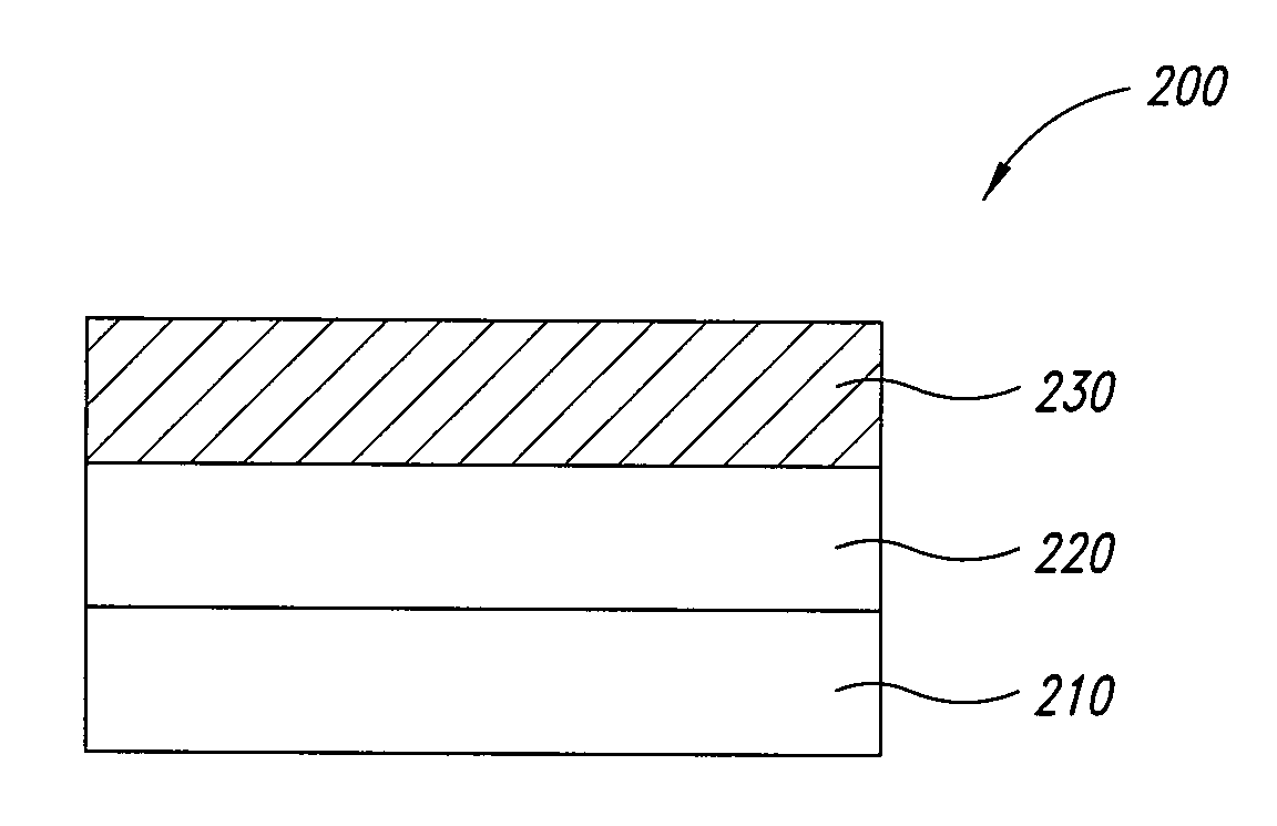
[0097]A coating solution was prepared by vigorously shaking 50% dispersion of ITO nanoparticles (Aldrich, Milwaukee, Wis.) in isopropyl alcohol (IPA) together with 50% silver nanowire dispersion of Example 2. The resulting coating solution was spin-coated onto a 2×2 inch Eagle glass substrate at 1000 rpm for 30 seconds. The coated substrate was then dried at 50° C. for 90 seconds and baked at 180° C. for 90 seconds. During coating and drying this mixture appeared to phase-separate into two layers; an underlying nanowire layer with good / low sheet resistance and an adjacent layer formed from the ITO nanoparticles that provided increased haze. The resulting conductive film had a transmission of 77%, a haze of 67% and a sheet resistance of 25Ω / □.


PUM

PropertyMeasurementUnit
hazeaaaaaaaaaa
sheet resistanceaaaaaaaaaa
hazeaaaaaaaaaa

Abstract

The present disclosure relates to modifications to nanostructure based transparent conductors to achieve increased haze / light-scattering with different and tunable degrees of scattering, different materials, and different microstructures and nanostructures.

Description

CROSS REFERENCE TO RELATED APPLICATION[0001]This application claims the benefit under 35 U.S.C. §119(e) of U.S. Provisional Application No. 61 / 266,945 filed Dec. 4, 2009, whereby this provisional application is incorporated herein by reference in its entirety.BACKGROUND[0002]Technical Field[0003]This disclosure generally relates to nanostructure-based transparent conductors having increased haze or light-scattering.[0004]Description of the Related Art[0005]Transparent conductors are optically clear and electrically conductive films. They are in widespread use in areas of display, touch-panel, photovoltaic (PV), various types of e-paper, electrostatic shielding, heating or anti-reflective coatings (e.g., windows), etc. Various technologies have produced transparent conductors based on one or more conductive media such as metallic nanostructures, transparent conductive oxides (TCO), conductive polymers, and / or carbon nanotubes.[0006]Depending on the end use, transparent conductors may...

Claims


Application Information

Patent Timeline
Patent Type & Authority Patents(United States)
IPC IPC(8): H01L31/0224B82Y20/00H01L31/0236H01L31/18
CPCB82Y20/00H01L31/0236H01L31/022466H01L31/1884Y02E10/50H01L29/413Y02E10/549H01B5/00H01B5/14H01L31/00H01L31/02168H01L31/04H10K30/10H10K30/82
Inventor BHATIA, RIMPLEPAKBAZ, HASHSEPA, JELENARAMOS, TERESAPSCHENITZKA, FLORIANSPAID, MICHAEL A.PICHLER, KARL
Owner CHAMP GREAT INTL
Why Eureka
Try Eureka