Pseudo tester-per-site functionality on natively tester-per-pin automatic test equipment for semiconductor test

a technology of automatic test equipment and test equipment, applied in the direction of electronic circuit testing, measurement devices, instruments, etc., can solve the problems of multi-site inefficiency, resource inefficiency, and waste of test resources, so as to reduce the number of test insertions, minimize test time, and reduce the effect of test insertions

Active Publication Date: 2017-03-28
ADVANTEST CORP
View PDF8 Cites 4 Cited by
  • Summary
  • Abstract
  • Description
  • Claims
  • Application Information

AI Technical Summary

Benefits of technology

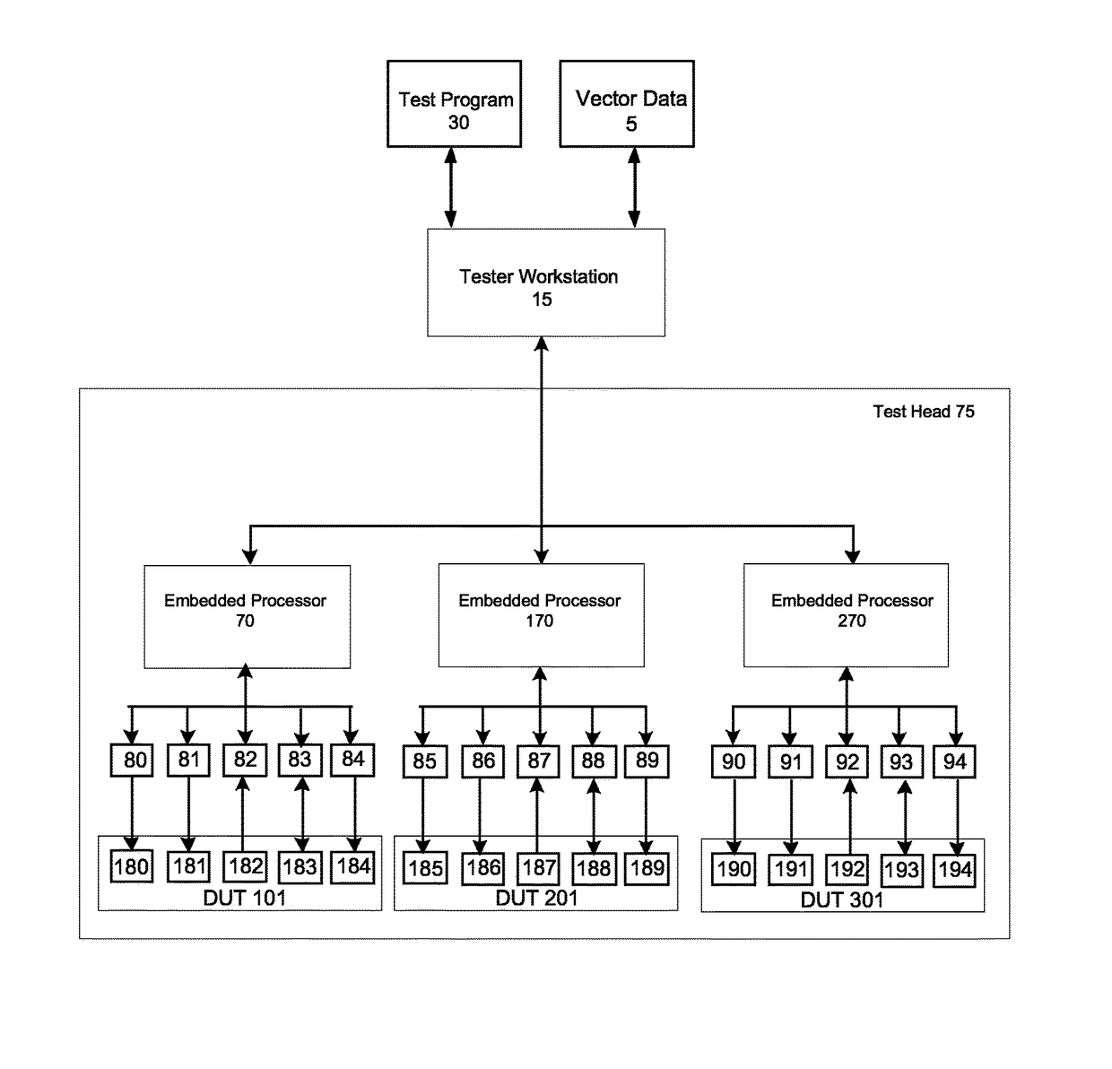
[0008]Embodiments of the present invention combine the TPS and TPP architectures by intelligently grouping TPP resources into pseudo test sites. This overcomes the limitations of either architecture on its own: Signal resources can be efficiently allocated for optimal signal integrity and load board routing while allowing per-site test program control to minimize test time. In this novel architecture, the test flow for each site is distributed to processing elements located within the test head.
[0009]By moving test program control down to embedded processors in the test head, the problems associated with multi-threading of test program control in the tester workstation are eliminated. The eases test program development, debug and maintenance. Multi-threading can only be done at the tester workstation level to support distributing test programs and vector data to the sites and collecting pass / fail data as tests complete.
[0010]Embodiments of the present invention also make it possible to reduce the number of test insertions needed to diagnose failed devices. Current industry practice has failed devices being sent back to Engineering, where they are re-installed on a tester to run additional testing in order to diagnose the failure in support of process or design improvements to increase test yield of the device. This novel architecture makes it possible to run additional testing on failed devices during the initial test insertion, making use of the tester time and resources that would otherwise be wasted as the failed device sits idle while other devices on the tester finish the complete test program.

Problems solved by technology

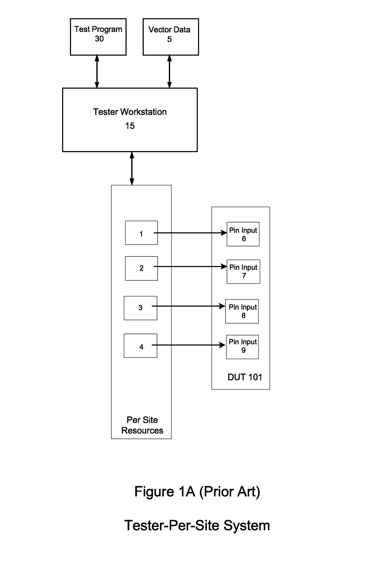
However, implementation of this architecture may also come at the expense of wasting testing resources since each resource cannot be shared among multiple sites during the test phase.
Furthermore, the TPS system's dedicated testing approach, in which all testing resources are focused on a single DUT, may result in wasted resources for devices that do not require those resources, thus resulting in resource inefficiencies.
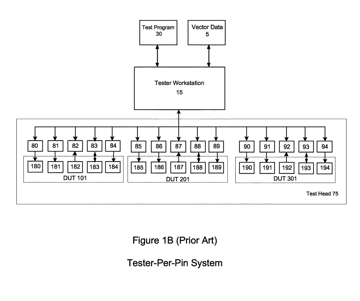
However, when testing in parallel under the TPP system, multi-site inefficiency problems exist.

Method used


Image

  • Pseudo tester-per-site functionality on natively tester-per-pin automatic test equipment for semiconductor test
  • Pseudo tester-per-site functionality on natively tester-per-pin automatic test equipment for semiconductor test
  • Pseudo tester-per-site functionality on natively tester-per-pin automatic test equipment for semiconductor test

Examples


Embodiment Construction

[0032]Reference will now be made in detail to the various embodiments of the present disclosure, examples of which are illustrated in the accompanying drawings. While described in conjunction with these embodiments, it will be understood that they are not intended to limit the disclosure to these embodiments. On the contrary, the disclosure is intended to cover alternatives, modifications and equivalents, which may be included within the spirit and scope of the disclosure as defined by the appended claims. Furthermore, in the following detailed description of the present disclosure, numerous specific details are set forth in order to provide a thorough understanding of the present disclosure. However, it will be understood that the present disclosure may be practiced without these specific details. In other instances, well-known methods, procedures, components, and circuits have not been described in detail so as not to unnecessarily obscure aspects of the present disclosure.

[0033]P...


PUM


Abstract

A system and method for testing devices are presented. Embodiments of the present invention use a central controller to coordinate the testing of a plurality of devices under test as well as a plurality of channel circuits that are each operable to be coupled to at least one I / O pin of a device under test of the aforementioned plurality of devices under test. Also, embodiments of the present invention include a plurality of intermediate processors that are each coupled to the central controller and operable to receive and send control signals. These intermediate processors are each coupled to a different set of channel circuits of the plurality of channel circuits and are operable to execute their own instantiation of a test program that is independent of any other intermediate processor of the plurality of intermediate processors for the testing of a device under test associated therewith.

Description

FIELD OF THE INVENTION[0001]Embodiments of the present invention generally relate to Automatic Test Equipment (ATE) for testing electronic components.BACKGROUND[0002]Automatic Test Equipment (ATE) is commonly used within the field of electrical chip manufacturing for the purposes of testing electronic components. ATE systems both reduce the amount of time spent on testing devices to ensure that the device functions as designed and serve as a diagnostic tool to determine the presence of faulty components within a given device before it reaches the consumer.[0003]Presently, there are two types of systems for testing system-on-chip semiconductor devices: Tester-Per-Site (TPS) and Tester-Per-Pin (TPP). The TPS system groups together a number of test functions that may be performed on each device under test (DUT) within what may be referred to as a “test site.” In a real time testing environment, a TPS system includes testing several DUTs on several test sites with one resource station a...

Claims


Application Information

Patent Timeline
Patent Type & Authority Patents(United States)
IPC IPC(8): G01R31/319
CPCG01R31/31907G01R31/31926
Inventor MOON, GERALDLEVENTHAL, IRA HARRISLARSON, RONKARAMCHANDANI, SANGEET
Owner ADVANTEST CORP
Why Eureka
Try Eureka