Eureka AIR delivers breakthrough ideas for toughest innovation challenges, trusted by R&D personnel around the world.

Integrated circuit cell library for multiple patterning

a technology of integrated circuits and cell libraries, applied in cad circuit design, originals for photomechanical treatment, instruments, etc., can solve the problems of large difference between the smallest wavelength and the smallest layout feature size, and the difficulty of lithographers patterning the layout feature size at 65 nm

Inactive Publication Date: 2017-04-25
RPX CORP
View PDF940 Cites 25 Cited by
  • Summary
  • Abstract
  • Description
  • Claims
  • Application Information

AI Technical Summary

Benefits of technology

The patent describes a method for designing a layout for an integrated circuit using a dynamic array architecture. The method involves creating a layout for a cell by defining a linear layout with a number of layout features that are commonly oriented. The layout is then split into smaller parts called sub-layouts, which can be independently fabricated. The method also includes a cell library that includes a definition of each cell, which includes the number of sub-layouts associated with each level of the cell. The layout features in the layout are organized in a consistent pattern across multiple cells, which helps in creating a chip-wide mask layout. The invention also provides a set of masks for fabricating a common level of a semiconductor chip. The technical effects of this invention include improved efficiency and accuracy in designing integrated circuits.

Problems solved by technology

However, as layout feature sizes continue to decrease without a corresponding decrease in available illumination wavelength, the difference between the smallest wavelength and smallest layout feature size has become too large for successful lithographic rendering of the features.
For example, lithographers are having great difficulty patterning 65 nm layout feature sizes with the 193 nm illumination source.

Method used


Image

  • Integrated circuit cell library for multiple patterning
  • Integrated circuit cell library for multiple patterning
  • Integrated circuit cell library for multiple patterning

Examples


Embodiment Construction

[0029]In the following description, numerous specific details are set forth in order to provide a thorough understanding of the present invention. It will be apparent, however, to one skilled in the art that the present invention may be practiced without some or all of these specific details. In other instances, well known process operations have not been described in detail in order not to unnecessarily obscure the present invention.

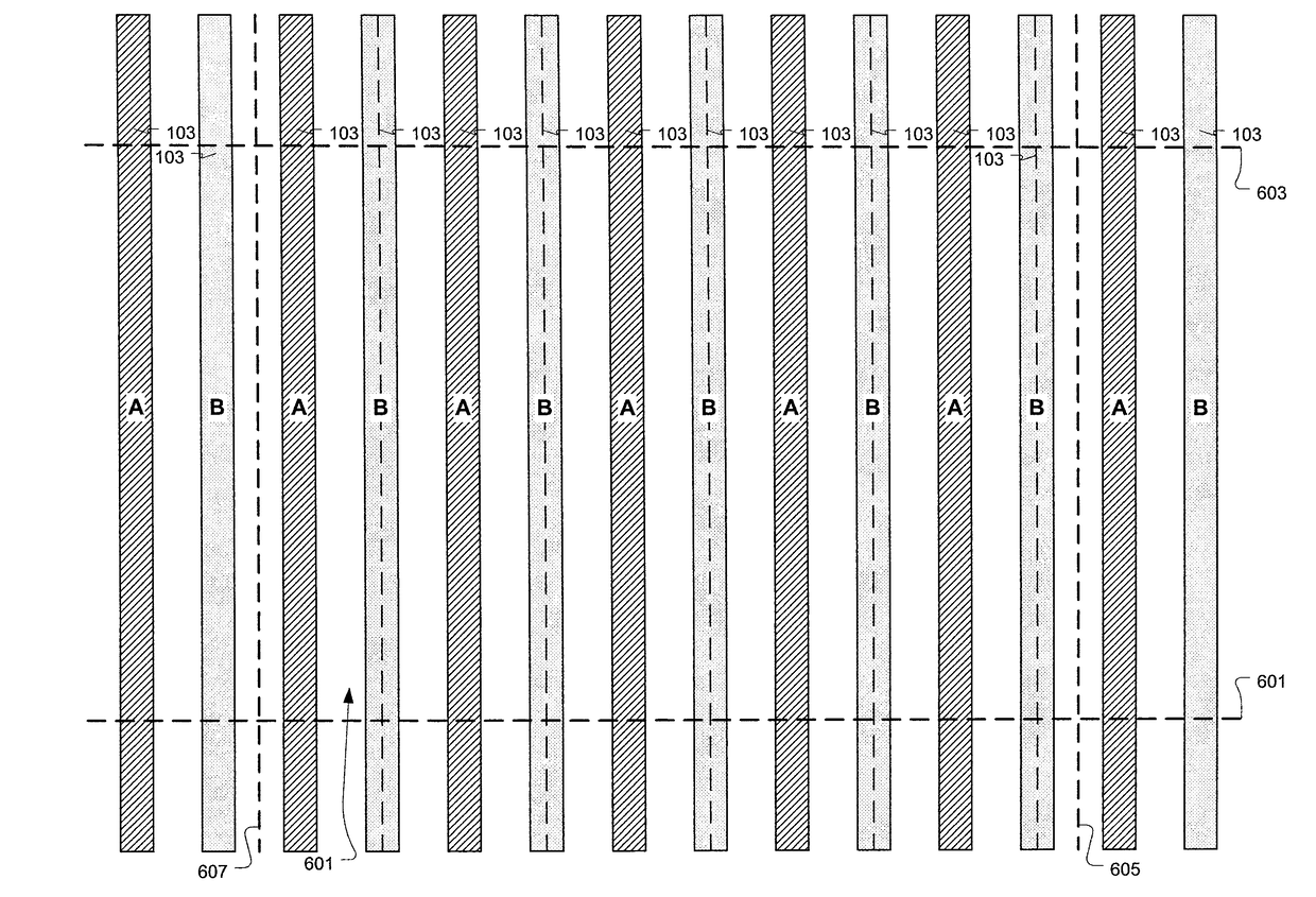
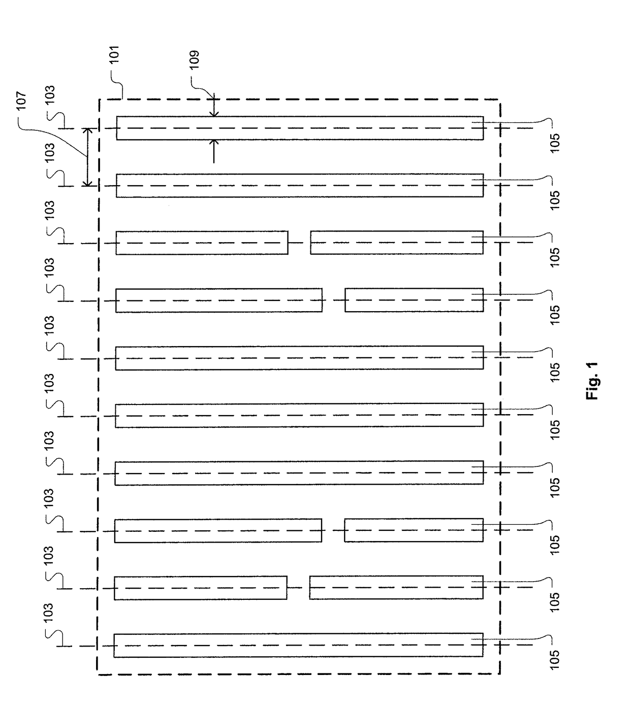
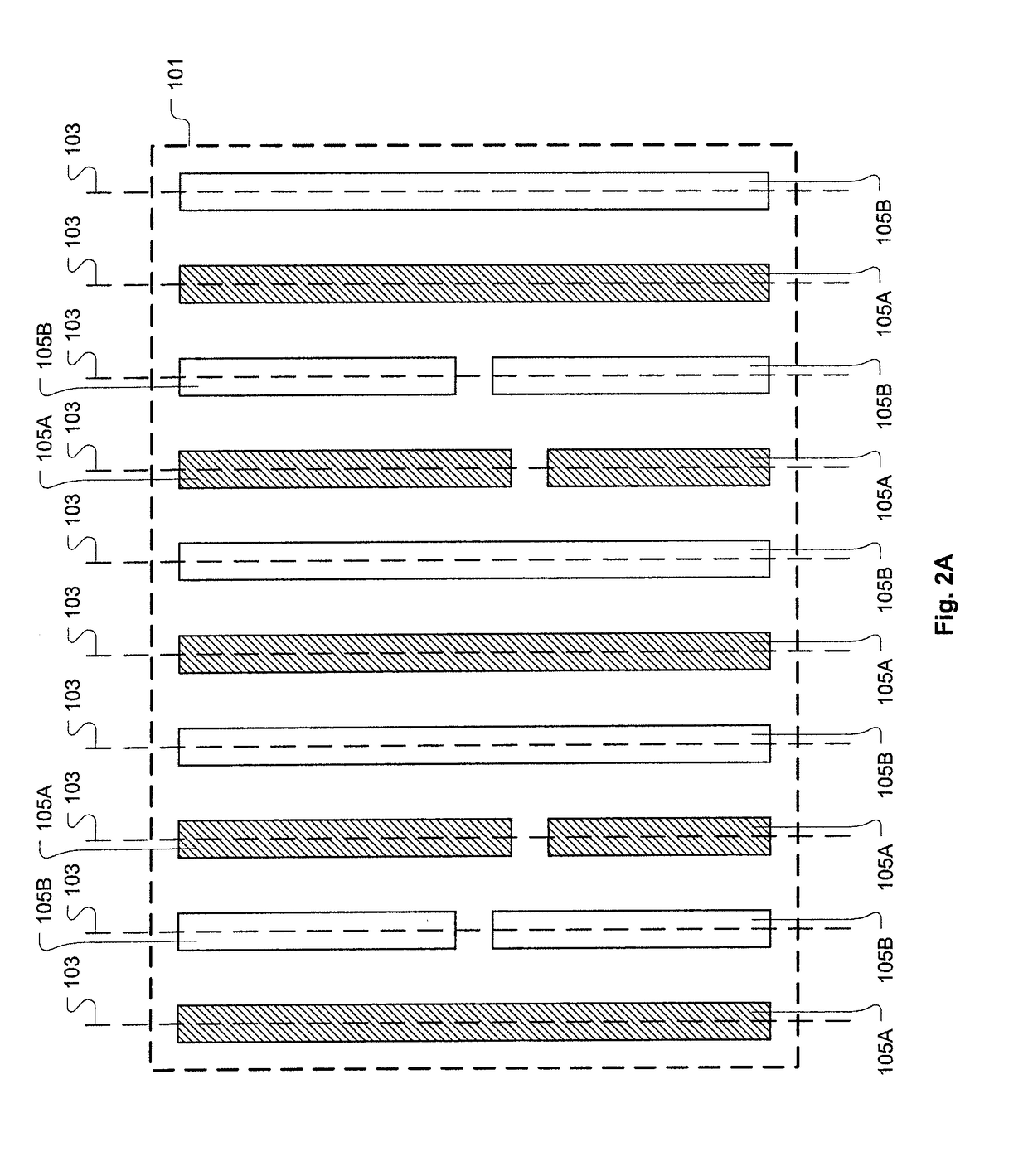
[0030]One technique for resolving nano-scale layout features without further decreasing the illumination wavelength and without further increasing the numerical aperture NA is to utilize multiple patterning. More specifically, in multiple patterning, a given layout is split into two or more sub-layouts that are each exposed separately over the same area of the chip in the optical lithography process. Although the individual feature sizes in each of the sub-layouts may be small, i.e., nano-scale, a spacing between adjacent layout features in a given sub-...


PUM

PropertyMeasurementUnit
wavelengthsaaaaaaaaaa

Abstract

A method is disclosed for defining a multiple patterned cell layout for use in an integrated circuit design. A layout is defined for a level of a cell in accordance with a dynamic array architecture so as to include a number of layout features. The number of layout features are linear-shaped and commonly oriented. The layout is split into a number of sub-layouts for the level of the cell. Each of the number of layout features in the layout is allocated to any one of the number of sub-layouts. Also, the layout is split such that each sub-layout is independently fabricatable. The sub-layouts for the level of the cell are stored on a computer readable medium.

Description

CLAIM OF PRIORITY[0001]This application is a continuation application under 35 U.S.C. 120 of prior U.S. patent application Ser. No. 12 / 041,584, filed on Mar. 3, 2008, which claims priority under 35 U.S.C. 119(e) to U.S. Provisional Patent Application No. 60 / 892,982, filed Mar. 5, 2007. The disclosures of the above-identified patent applications are incorporated herein by reference in their entirety.CROSS-REFERENCE TO RELATED APPLICATIONS[0002]This application is also related to U.S. patent application Ser. No. 11 / 683,402, filed on Mar. 7, 2007, and entitled “Dynamic Array Architecture.” This application is also related to U.S. patent application Ser. No. 12 / 013,342, filed on Jan. 11, 2008, and entitled “Semiconductor Device with Dynamic Array Section.” This application is also related to U.S. patent application Ser. No. 12 / 013,356, filed on Jan. 11, 2008, and entitled “Methods for Designing Semiconductor Device with Dynamic Array Section.” This application is also related to U.S. pa...

Claims


Application Information

Patent Timeline
Patent Type & Authority Patents(United States)
IPC IPC(8): G06F17/50H01L27/02H01L27/00G03F1/70H01L27/118
CPCH01L27/0207G03F1/70G06F17/5068G06F17/5072G06F17/5077H01L27/11807G06F30/39G06F30/392G06F30/394G06F2119/18G06F30/3947
Inventor SMAYLING, MICHAEL C.BECKER, SCOTT T.
Owner RPX CORP
Why Eureka
Eureka Blog
Learn More