Electrode sheet for capacitance-type touch panel
a capacitance-type touch panel and electrode-type technology, applied in the field of electrode-type touch panel electrode-type electrode-type sheet, can solve the problems of multi-touch, response speed, and reduced current transfer rate between electrodes, and achieve the effect of high transparency
- Summary
- Abstract
- Description
- Claims
- Application Information
AI Technical Summary
Benefits of technology
Problems solved by technology
Method used
Image
Examples
first embodiment
[0043](Constitution of an Electrode Sheet)
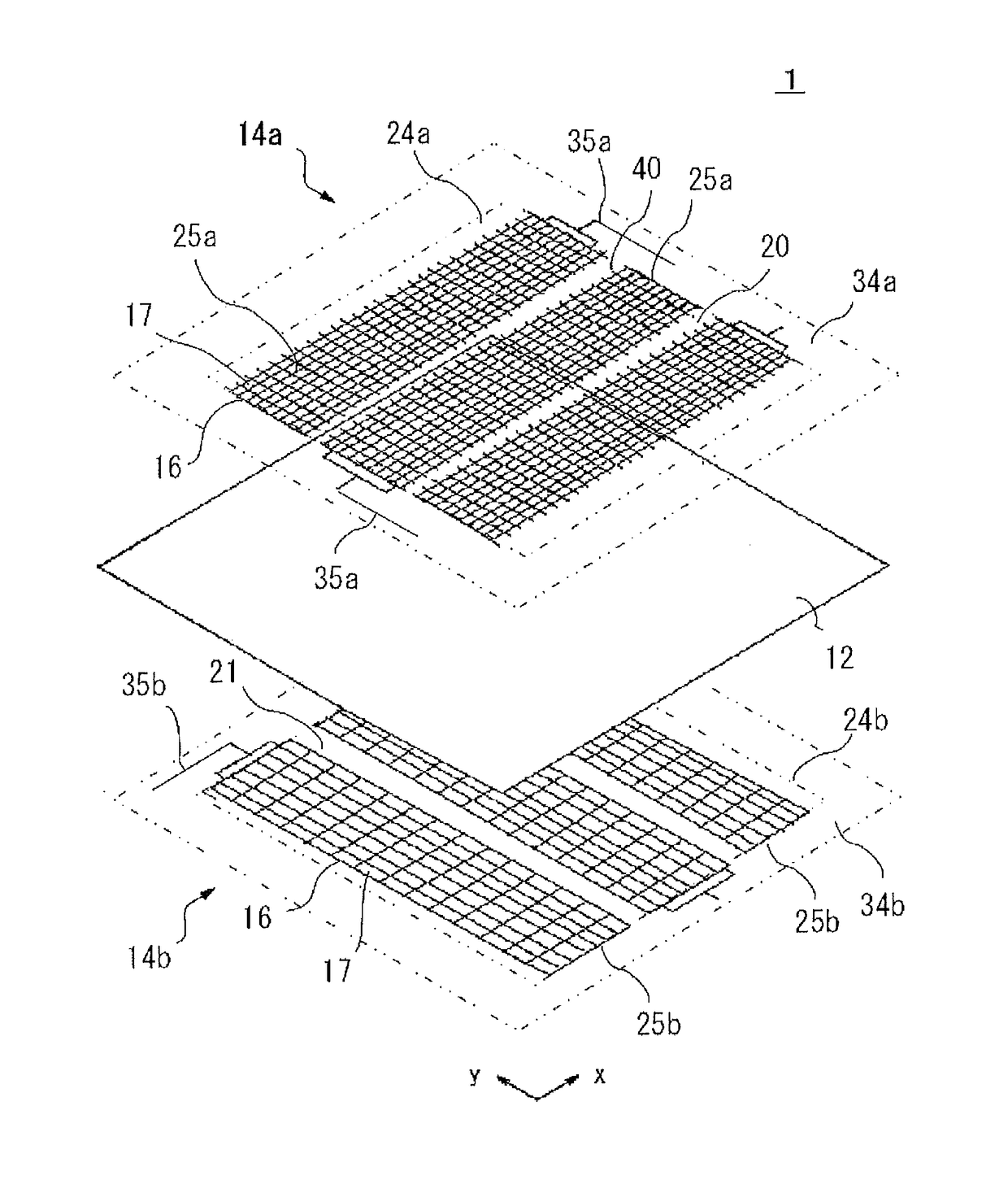
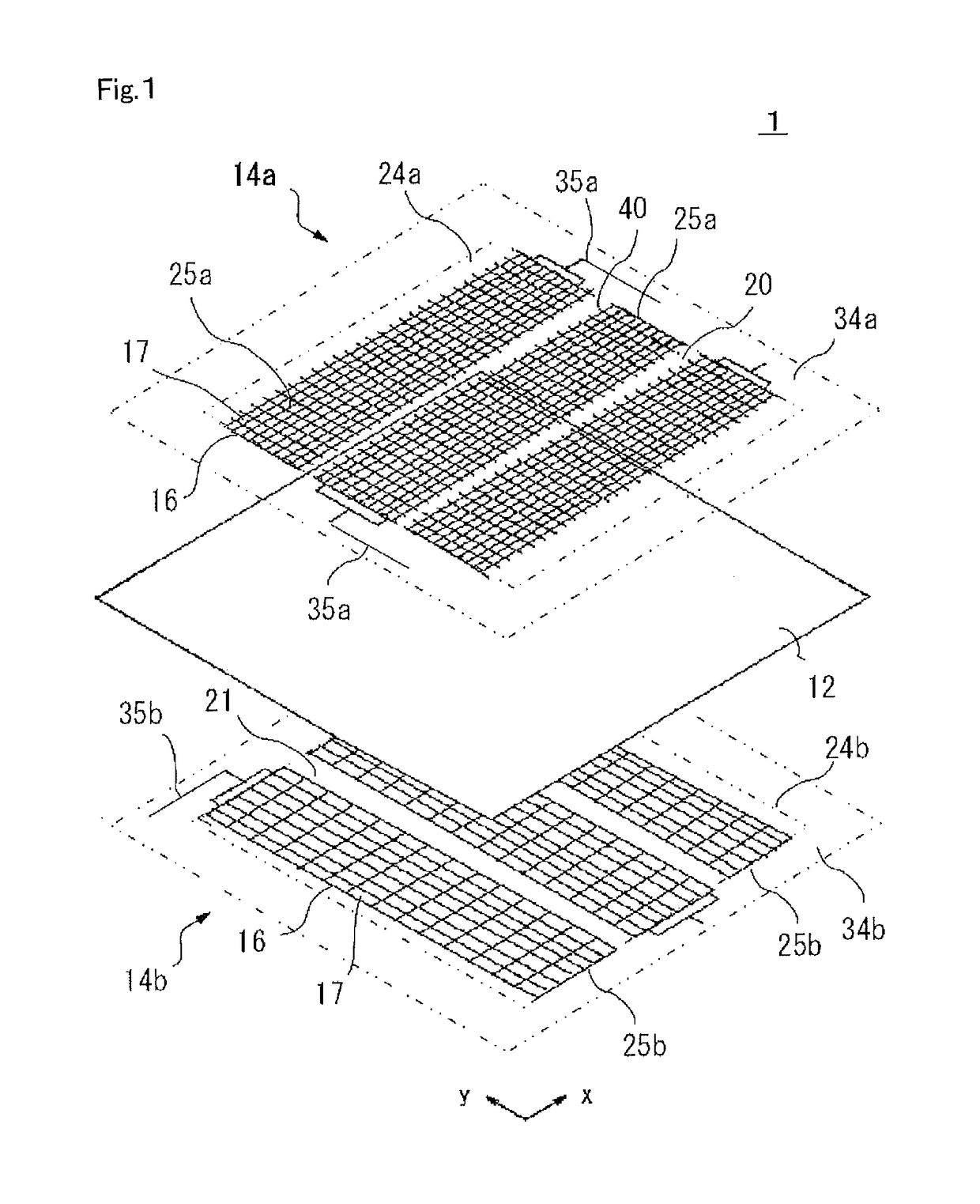
[0044]An electrode sheet for a capacitance-type touch panel of a first embodiment comprises a transparent substrate 12, a first conductive part 14a provided on one principal surface of the substrate 12, and a second conductive part 14b provided on the other principal surface of the substrate 12, as shown in FIG. 1. FIG. 2 shows a cross-sectional view of one of a first electrode pattern 25a in the electrode sheet shown in FIG. 1 across a longitudinal direction thereof.
[0045]The substrate 12 is made of a material having an insulating property and high translucency, such as resins, glasses and silicone. Examples of the resin include polyesters such as polyethylene terephthalate (PET), polylactic acid (PLA) and polyethylene naphthalate (PEN), polyolefins such as polyethylene (PE), polypropylene (PP), polystyrene, EVA, cycloolefin polymer (COP) and cyclic olefin copolymer (COC), and others such as vinyl resins, polycarbonate (PC), polyamides, pol...
second embodiment
[0095]In the first embodiment, each of the first electrode pattern 25a and the second electrode pattern 25b has a mesh structure; however, the first electrode pattern 25a and the second electrode pattern 25b are not limited to the mesh structure as long as they are composed of an opaque conductive fine line 16 and a blank part 17 partitioned by the conductive fine line. For example, the second electrode pattern 25b may be formed in a comb-shape in which teeth are arranged in X direction as shown in FIG. 9 (second embodiment), instead of the mesh structure. FIG. 10 shows a cross-sectional view of one of the first electrode pattern 25a in the electrode sheet shown in FIG. 9 across the longitudinal direction thereof.
[0096]In FIG. 9, the line segments 16a facing across the substrate 12 are comprised from teeth of the comb-shape in the second electrode pattern 25b. In the conductive fine line of the first electrode pattern 25a, only a part of the outline of the quadrangle that forms the ...
third embodiment
[0101]In the first embodiment, nothing is provided at the gap 20 between the adjacent first electrode patterns 25a and the gap 21 between the adjacent second electrode patterns 25b in the first conductive part 14a and the second conductive part 14b; however, the present invention is not limited thereto. For example, as shown in FIG. 13, the first conductive part 14a has a plurality of first dummy patterns 55a, that are composed of a conductive fine line 18 made of the same material as the first electrode pattern 25a, placed at the gap 20 between the adjacent first electrode patterns 25a, and insulated electrically from the first electrode pattern 25a; and the second conductive part 14b has a plurality of second dummy patterns 55b, that are composed of a conductive fine line 18 made of the same material as the second electrode pattern 25b, placed at the gap 21 between the adjacent second electrode patterns 25b, and insulated electrically from the second electrode pattern 25b (third e...
PUM
 Abstract
Description
Claims
Application Information


