Supercharge Your Innovation With Domain-Expert AI Agents!

Pixel defining layer, organic electroluminescent device and display device

a technology of electroluminescent devices and defining layers, applied in the field of display technology, can solve the problems of low material utilization, inability to manufacture large-sized products, and inability to produce large-scale products, and achieve the effect of effective cost reduction and improved production efficiency

Active Publication Date: 2017-06-13
BOE TECH GRP CO LTD
View PDF13 Cites 0 Cited by
  • Summary
  • Abstract
  • Description
  • Claims
  • Application Information

AI Technical Summary

Benefits of technology

[0025]The present invention provides a pixel defining layer, an organic electroluminescent device and a display device with the following advantages:
[0027](2) the making of the double-layered pixel defining layer omits the process of using two masks, which can effectively reduce costs and improve production efficiency.

Problems solved by technology

(1) a vacuum deposition process which is applicable to small organic molecules and characterized in that an organic film can be formed without a solvent to have a uniform thickness, but with disadvantages of high equipment investment, low material utilization and incapability of manufacturing large-sized products; and
(2) solution-related method, including spin coating, ink-jet printing, nozzle coating method, applicable to polymer materials and small soluble molecules, which is characterized by low equipment costs, and prominent performance on large-scale, large-sized production. In particular, the ink-jet printing technology enables a solution to be precisely ink-jetted into a pixel region to thereby form an organic film. But the biggest difficulty lies in that the organic solution in the pixel area can hardly form an organic film having a uniform thickness.

Method used


Image

  • Pixel defining layer, organic electroluminescent device and display device
  • Pixel defining layer, organic electroluminescent device and display device
  • Pixel defining layer, organic electroluminescent device and display device

Examples


Embodiment Construction

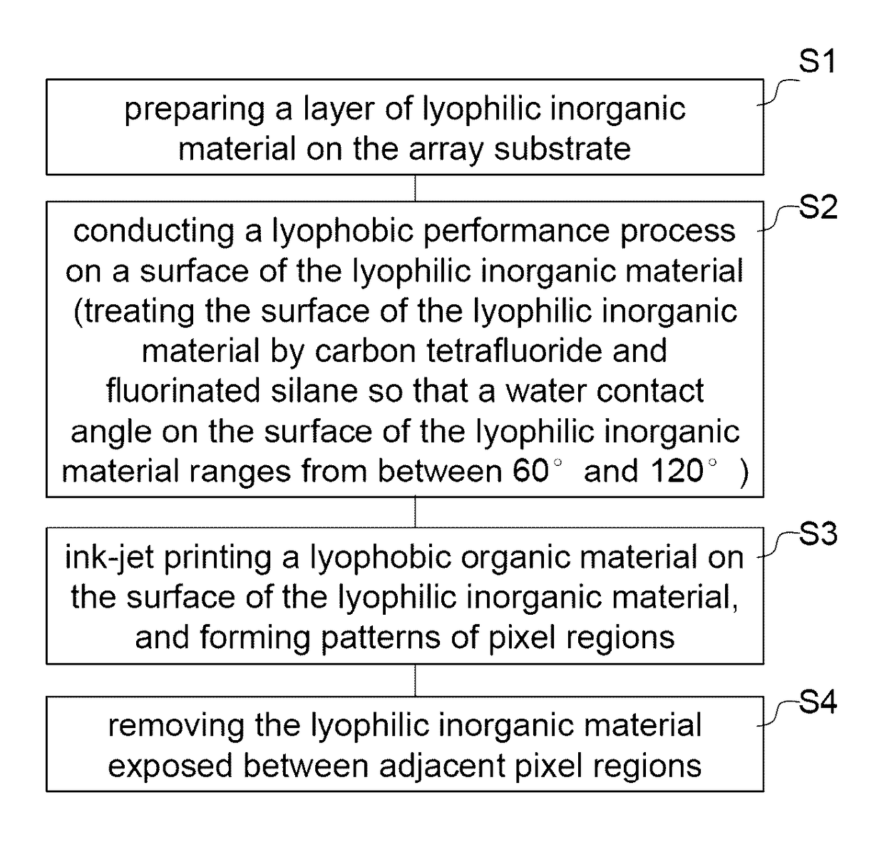
[0031]The embodiments of the present invention will be further described in detail with reference to the drawings and examples. The following examples are used to explain the present invention, rather than limit the scope of the present invention.

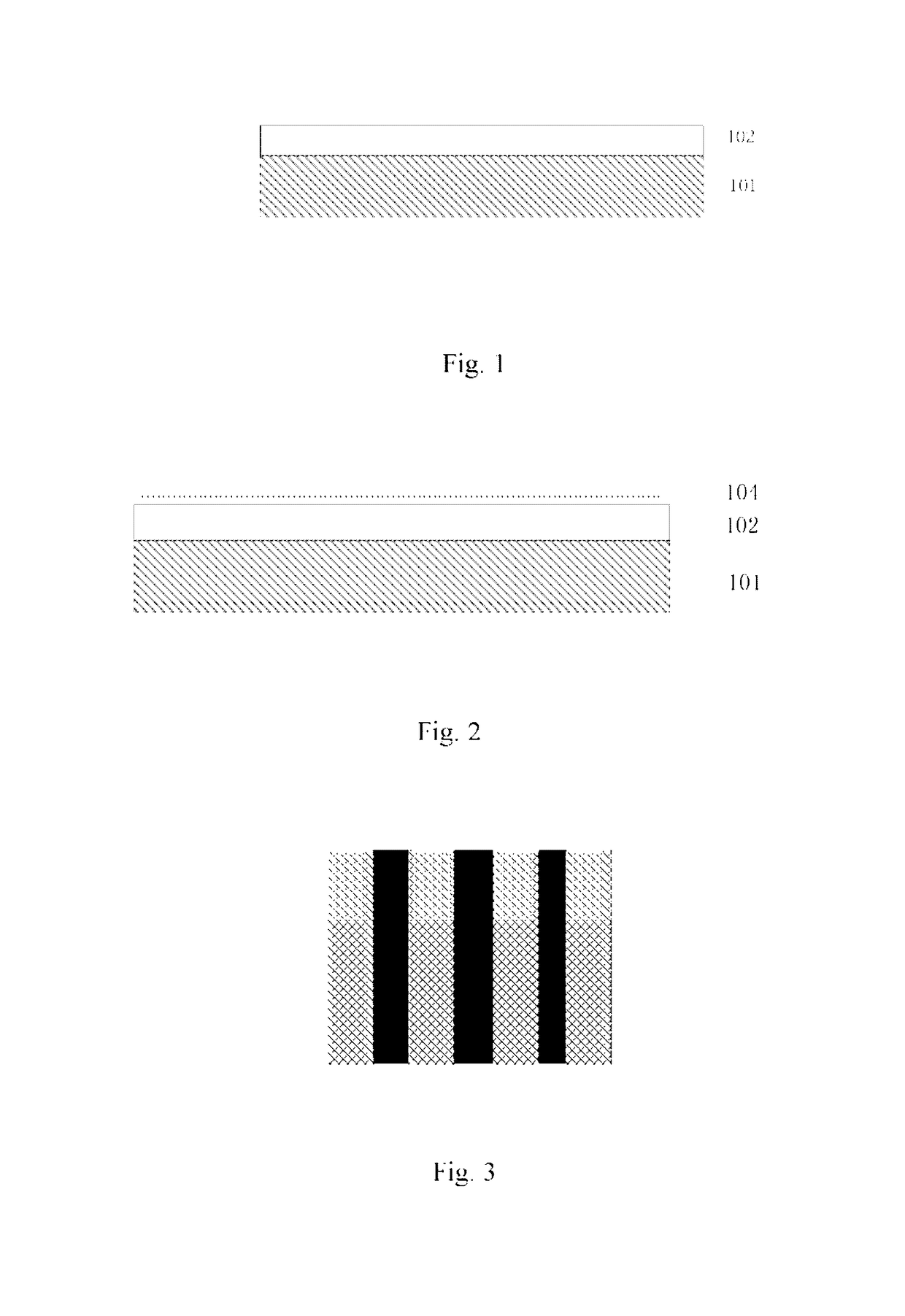
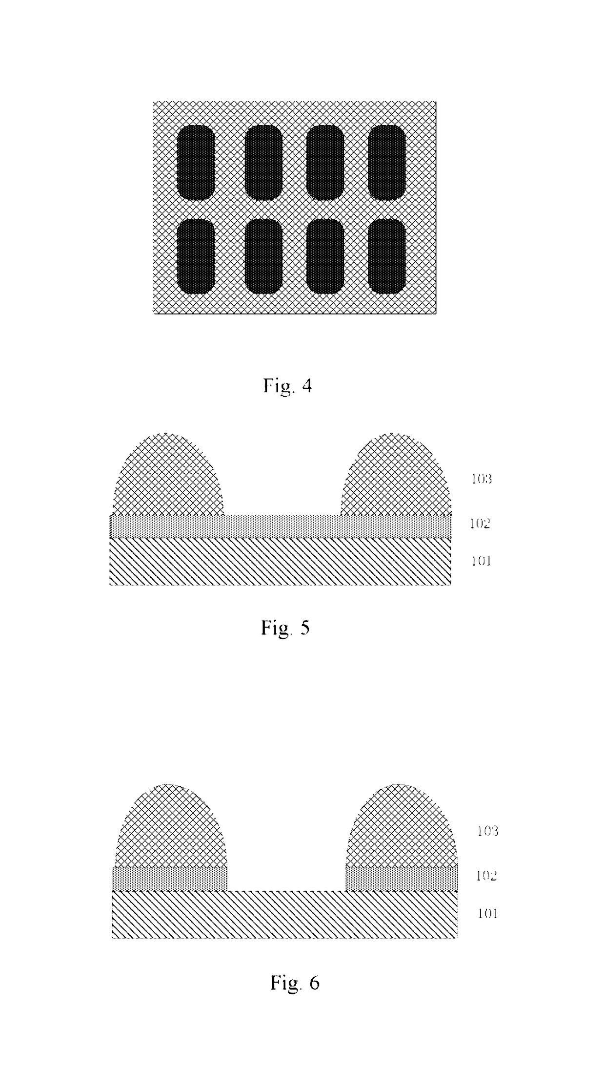
[0032]As shown in FIG. 6, the example of the present invention provides a pixel defining layer, comprising a first defining layer 102 on an array substrate 101 and a second defining layer 103 on the first defining layer;

[0033]The first defining layer 102 is made of a lyophilic inorganic material; The second defining layer 103 is made of a lyophobic organic material.

[0034]The lyophilic inorganic material preferably comprises SiO2 or SiNx, and the lyophobic organic material preferably comprises a polyimide photoresist, an acrylic-like photoresist and an organic insulating material.

[0035]Furthermore, the present invention also provides an organic electroluminescent device comprising the pixel defining layer as described above.

[0036]In addition...


PUM


Abstract

The present invention relates to the field of display technology, particularly to a pixel defining layer, an organic electroluminescent device and a display device. The pixel defining layer comprises a first defining layer on an array substrate and a second defining layer on the first defining layer, wherein the first defining layer is made of a lyophilic inorganic material, and the second defining layer is made of a lyophobic organic material. The present invention provides a pixel defining layer, an organic electroluminescent device and a display device, wherein ink-jet printing technology is used to patternize pixels of an organic material, which serves as not only a protective layer on the first inorganic material layer during dry etching, but also a lyophobic layer on the second layer; the making of the double-layered pixel defining layer omits the process of using two masks, which can effectively reduce costs and improve production efficiency.

Description

CROSS-REFERENCE TO RELATED APPLICATIONS[0001]The present application is the U.S. national phase entry of PCT / CN2015 / 071609, filed on Jan. 27, 2015 which claims the benefit of Chinese Patent Application No. 201410601922.8, filed on Oc. 30, 2014, the entire disclosures of which are incorporated herein by reference.FIELD OF THE INVENTION[0002]The present invention relates to the field of display technology, particularly to a pixel defining layer, an organic electroluminescent device and a display device.BACKGROUND OF THE INVENTION[0003]In relation to OLED (Organic Light-Emitting Diode) or PLED (Polymer Light-Emitting Diode), the method for forming an organic film includes:[0004](1) a vacuum deposition process which is applicable to small organic molecules and characterized in that an organic film can be formed without a solvent to have a uniform thickness, but with disadvantages of high equipment investment, low material utilization and incapability of manufacturing large-sized product...

Claims


Application Information

Patent Timeline
Patent Type & Authority Patents(United States)
IPC IPC(8): H01L27/32H01L51/52H01L51/56
CPCH01L27/3246H01L27/3283H01L51/52H01L51/56H01L2227/323H10K59/88H10K50/11H10K50/80H10K2102/302H10K71/00H10K59/173H10K59/122H10K59/1201
Inventor HOU, WENJUNLIAO, CHINLUNGLIU, ZE
Owner BOE TECH GRP CO LTD
Features
  • R&D
  • Intellectual Property
  • Life Sciences
  • Materials
  • Tech Scout
  • Unparalleled Data Quality
  • Higher Quality Content
  • 60% Fewer Hallucinations
Learn More