
Display device and method of manufacturing the same

a technology of a display device and a manufacturing method, which is applied in the manufacture of electrode systems, electric discharge tubes/lamps, instruments, etc., can solve the problem of not considering the possibility of reducing moisture intrusion from the cut seal, and achieve the effect of reducing moisture intrusion

Inactive Publication Date: 2017-08-22
JAPAN DISPLAY INC
View PDF16 Cites 2 Cited by
  • Summary
  • Abstract
  • Description
  • Claims
  • Application Information

AI Technical Summary

Benefits of technology

The present invention provides a display device with reduced moisture intrusion from the seal. This is achieved by incorporating a low moisture-permeable layer on the seal and at least one projecting stripe portion on the substrate, which helps to thin the seal and reduce moisture intrusion. The method for manufacturing the display device involves cutting the mother substrates to form the plurality of spaces for arranging the element for displaying an image, with the seal being placed between adjacent spaces and the low moisture-permeable layer being laminated on the seal in the region between adjacent spaces. The cutting process also results in an exposed surface on the low moisture-permeable layer, which further reduces moisture intrusion.

Problems solved by technology

However, no consideration is made of reducing moisture intrusion from the cut seal.

Method used


Image

  • Display device and method of manufacturing the same
  • Display device and method of manufacturing the same
  • Display device and method of manufacturing the same

Examples


Embodiment Construction

[0024]In the following, an embodiment of the present invention is described with reference to the drawings.

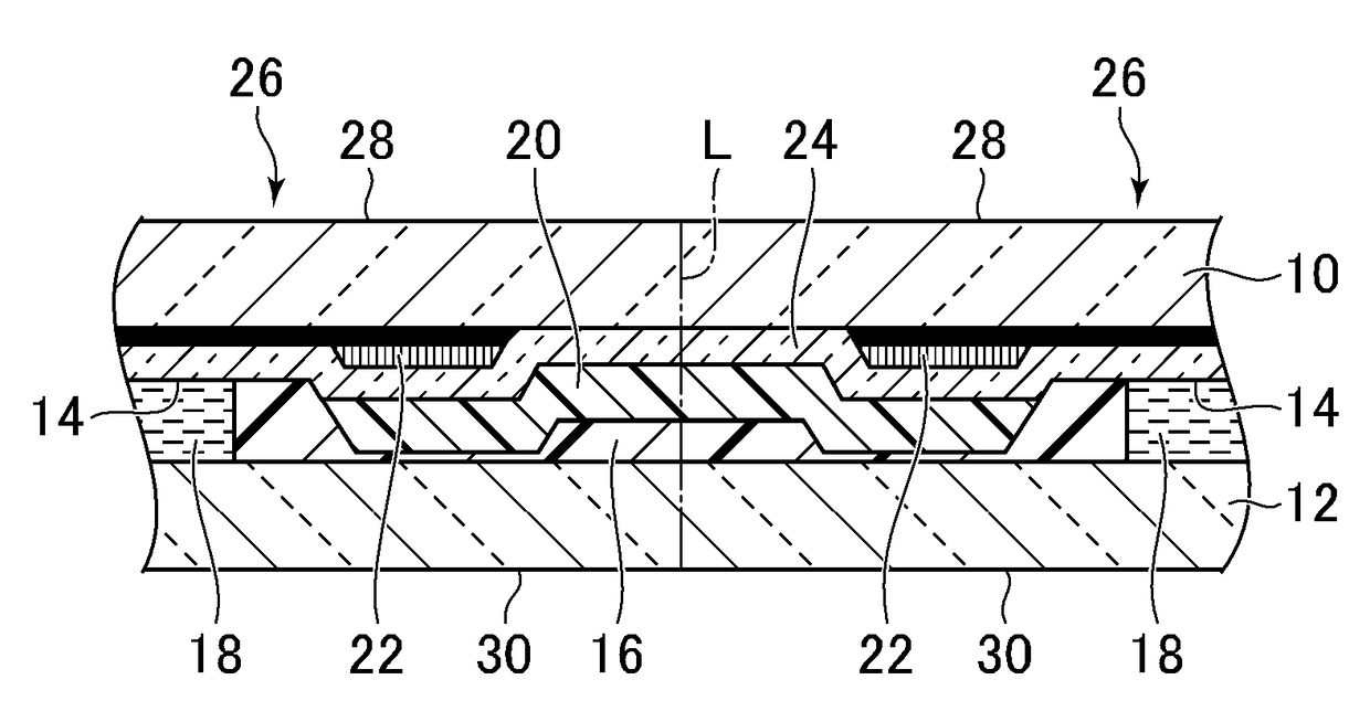
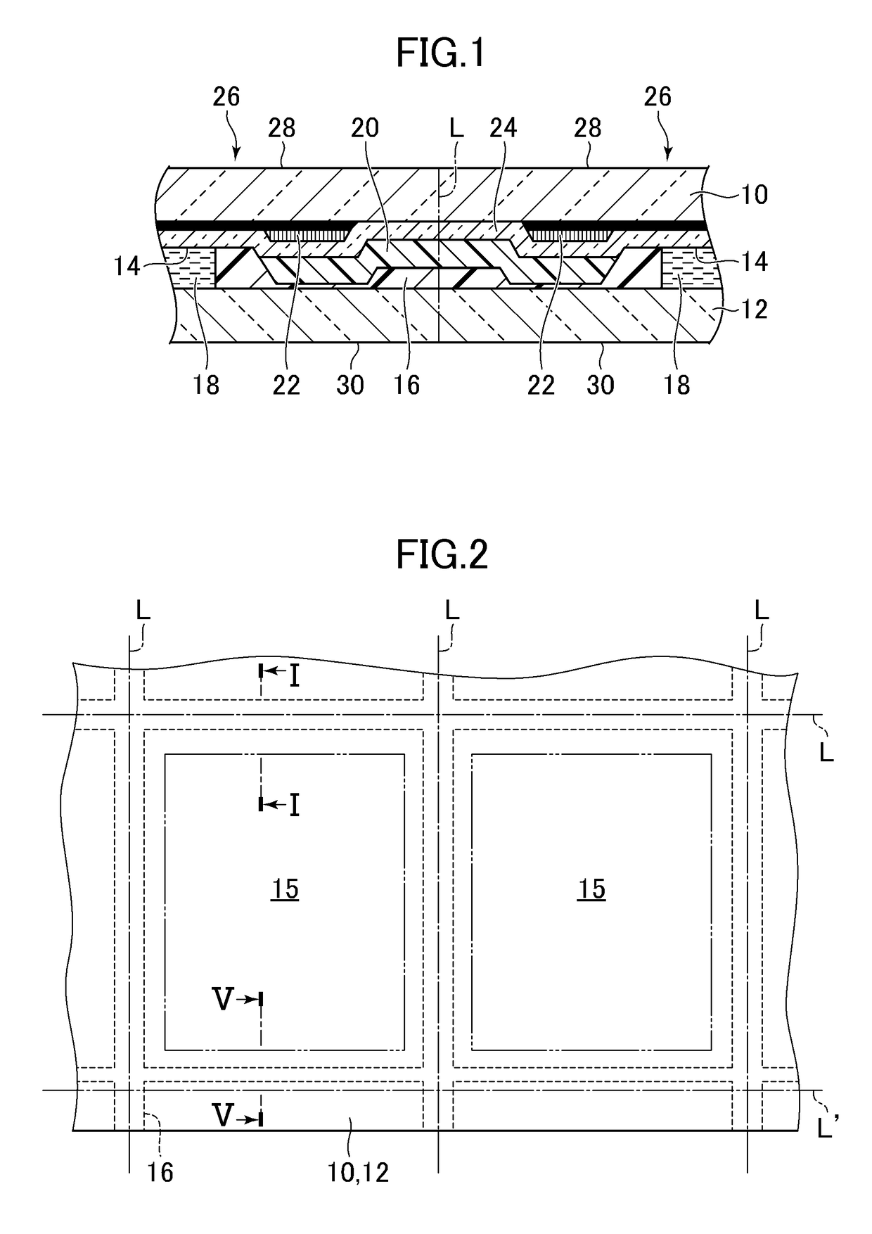
[0025]FIG. 1 is a view illustrating a method of manufacturing a display device according to the embodiment of the present invention. The display device manufactured in this embodiment is a liquid crystal display device, but the present invention is applicable to other display devices such as an organic electroluminescence device.

[0026]In this embodiment, a pair of mother substrates 10 and 12 is prepared. FIG. 1 illustrates a cross-section of the pair of mother substrates 10 and 12. The mother substrate 10 is a color filter substrate in which a color filter is formed. Specifically, the mother substrate 10 includes a plurality of integrated color filter substrates as components of a plurality of display devices, and is cut into a plurality of individual pieces in the subsequent step. The mother substrate 10 is made of a light-permeable material such as glass. The mother substrate...


PUM

PropertyMeasurementUnit
moisture permeabilityaaaaaaaaaa
lengthaaaaaaaaaa
permeableaaaaaaaaaa

Abstract

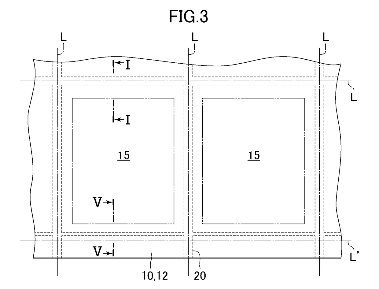
Between a pair of mother substrates, spaces are defined by a seal. The pair of mother substrates is cut to cut out cells. The seal is arranged to fill a region between adjacent spaces. On the seal, a low moisture-permeable layer made of a material that is harder and has lower moisture permeability than the seal is laminated in the region between the adjacent spaces. On at least one of the pair of mother substrates, a pair of projecting stripe portions extending along a length of the seal and arranged at an interval is formed in the region between the adjacent spaces at a position overlapping with the seal and the low moisture-permeable layer. In a step of cutting the pair of mother substrates, together with the pair of mother substrates, the seal and the low moisture-permeable layer are cut between the pair of projecting stripe portions.

Description

CROSS-REFERENCE TO RELATED APPLICATION[0001]The present application claims priority from Japanese application JP 2011-233832 filed on Oct. 25, 2011 the content of which is hereby incorporated by reference into this application.BACKGROUND OF THE INVENTION[0002]1. Field of the Invention[0003]The present invention relates to a display device and a method of manufacturing the same.[0004]2. Description of the Related Art[0005]As a method of manufacturing a display panel, there is known a method of cutting out individual display panels from large-sized mother glass substrates. A liquid crystal display panel has a structure in which liquid crystal is sealed by a seal between a pair of substrates. Therefore, by cutting the mother glass substrates while avoiding the seal, the mother glass substrates are prevented from being broken due to cutting force dispersion.[0006]In recent years, there has been a demand for narrowing an outer region (frame) of a display region of the display panel, and ...

Claims


Application Information

Patent Timeline
Patent Type & Authority Patents(United States)
IPC IPC(8): G02F1/1339G02F1/1333
CPCG02F1/1339G02F1/133351H05B33/04
Inventor TANIGUCHI, JIRONAGAMI, TAKAHIRO
Owner JAPAN DISPLAY INC
Learn More