
Laminated coil component and matching circuit

a technology of laminated coils and components, applied in the direction of impedence networks, transformers/inductance details, inductances, etc., can solve the problems of unnecessary coupling between deterioration of characteristics due to unnecessary coupling between adjacent components, and unnecessary coupling of coils and conductor layers, etc., to achieve high accuracy

Active Publication Date: 2017-11-07
MURATA MFG CO LTD
View PDF13 Cites 0 Cited by
  • Summary
  • Abstract
  • Description
  • Claims
  • Application Information

AI Technical Summary

Benefits of technology

[0007]In view of the above, preferred embodiments of the present invention provide a laminated coil component capable of significantly reducing or preventing the unnecessary coupling between a plurality of coils while the coils are proximally arranged, and also a matching circuit provided with such a laminated coil component.
[0010]The outline of the first coil conductor pattern, in a plan view, may preferably overlap the outline of the second coil conductor pattern. This configuration enables both of the first coil conductor pattern and the second coil conductor pattern to define a coil of which the opening has a large diameter, in a limited space. In other words, in order to significantly reduce or prevent coupling, a coil having a small diameter does not need to be defined and thus the configuration makes it possible to configure a coil having necessary inductance with the small number of turns.
[0018]According to various preferred embodiments of the present invention, while the interlayer distance between the first coil conductor pattern and the second coil conductor pattern is small, the coil defined by the first coil conductor pattern and the coil defined by the second coil conductor pattern is able to be in an uncoupled state or in a relatively weakly coupled state. Thus, the interlayer distance between the first coil conductor pattern and the second coil conductor pattern is significantly reduced and a plurality of coils are arranged in a limited space. Moreover, even if the interlayer distance is small, the degree of coupling of the coil defined by the first coil conductor pattern and the coil defined by the second coil conductor pattern is able to be determined with high accuracy.

Problems solved by technology

However, with the mounting in the proximity state, the deterioration of the characteristics due to unnecessary coupling between adjacent components becomes a problem.
As disclosed in Japanese Unexamined Patent Application Publication No. 11-016738, in the structure in which a ground conductor layer is inserted between the layers of each coil conductor pattern, the coils and the conductor layers are likely to be unnecessarily coupled to each other and the unnecessary coupling deteriorates the Q value of the coils.
Therefore, the coil conductor pattern and the ground conductor layer still require a large space between the coil conductor pattern and the ground conductor layer.

Method used


Image

  • Laminated coil component and matching circuit
  • Laminated coil component and matching circuit
  • Laminated coil component and matching circuit

Examples


first preferred embodiment

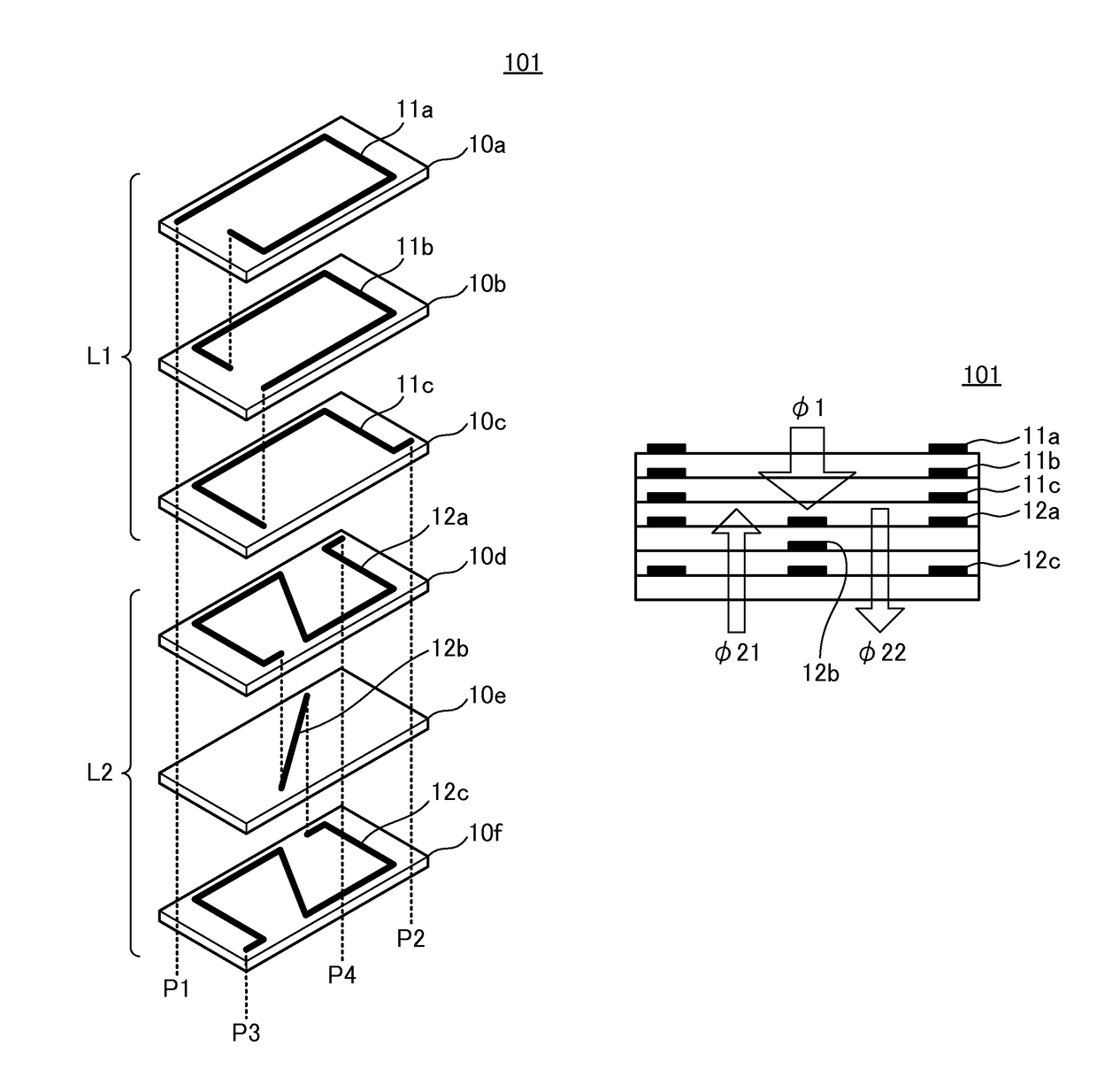
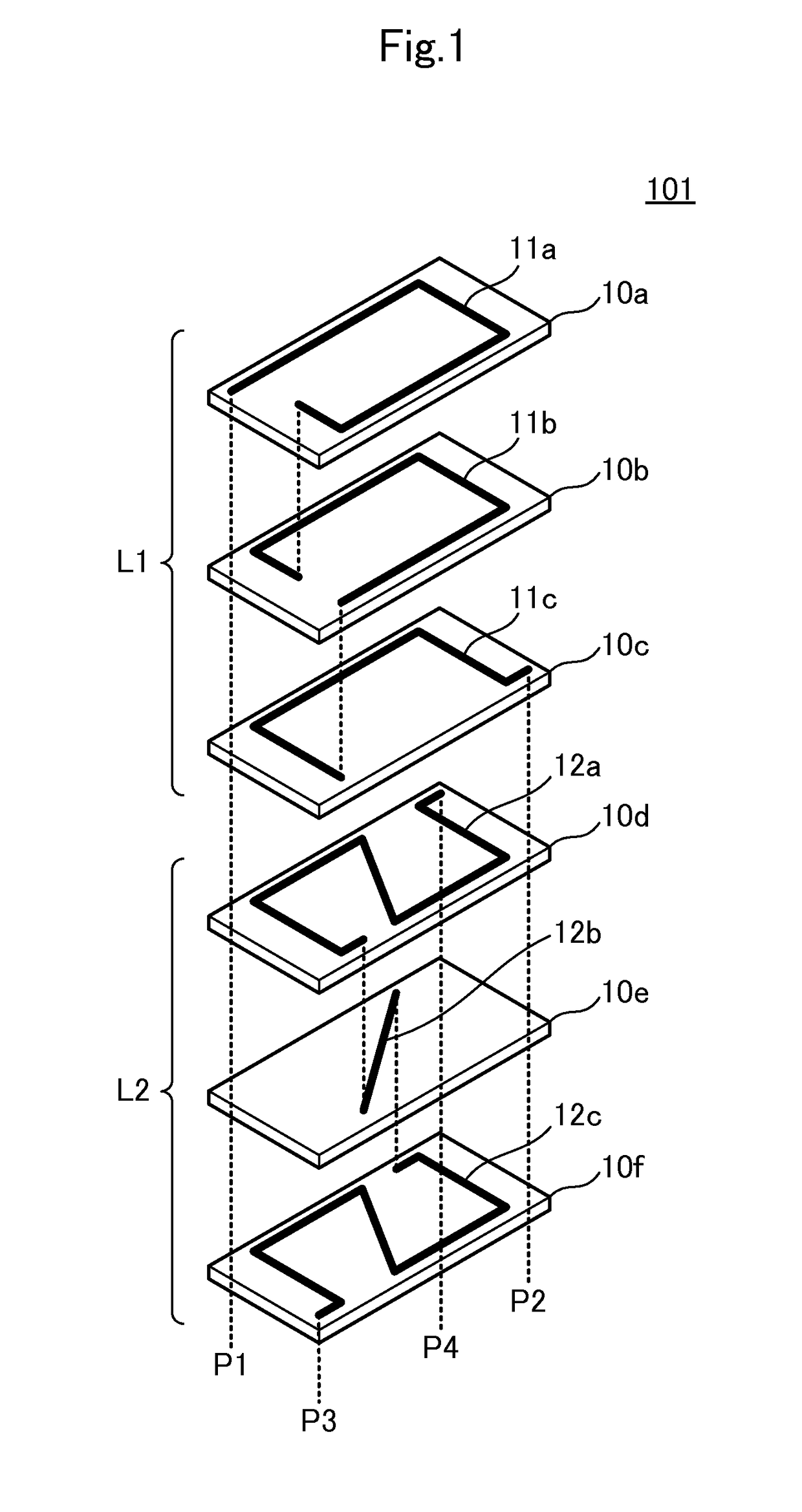
[0040]FIG. 1 is an exploded perspective view of a main portion of a laminated coil component 101 according to a first preferred embodiment of the present invention.

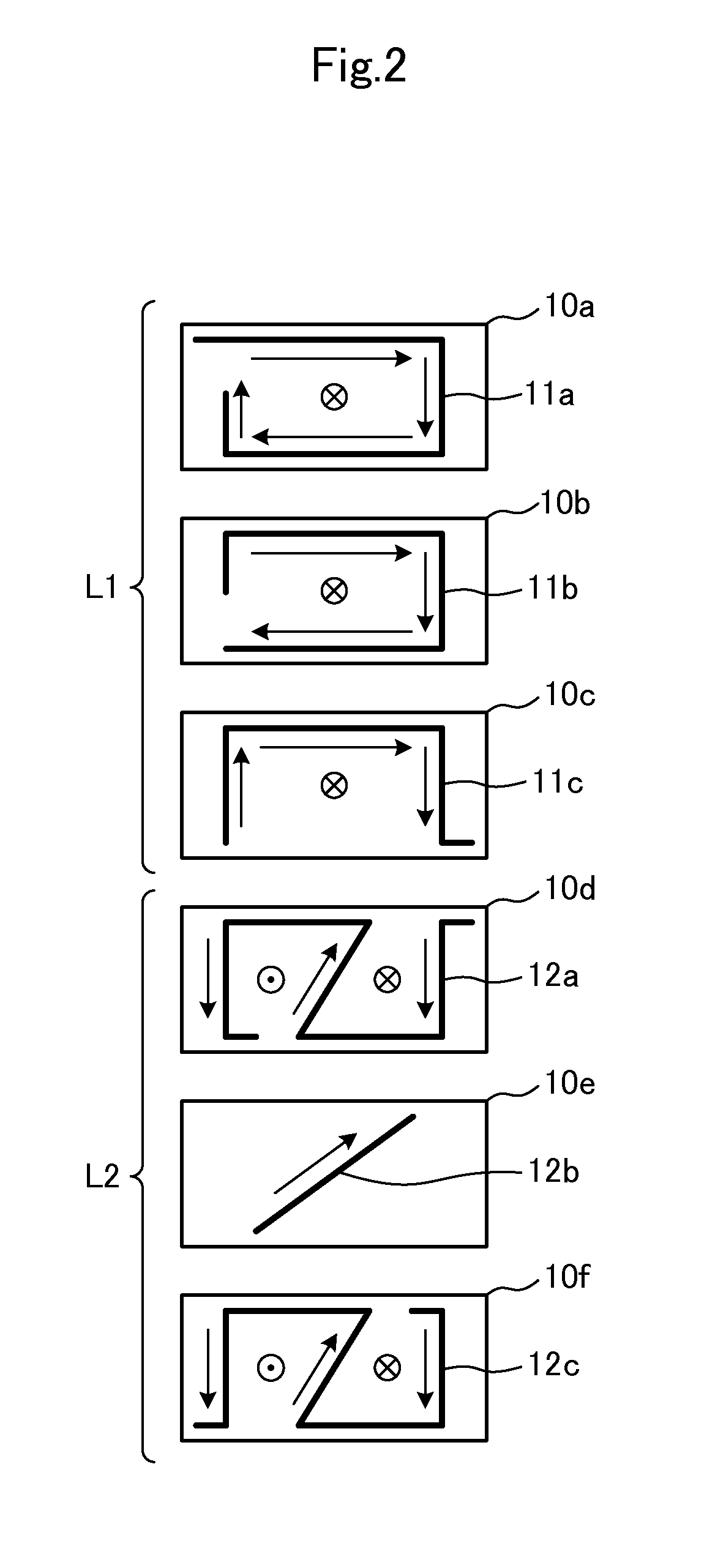
[0041]The laminated coil component 101 includes insulating layers 10a to 10f that are laminated on each other, each of the insulating layers 10a to 10f including at least one conductor pattern; and at least one coil defined by the conductor patterns. The conductor patterns include first coil conductor patterns 11a, 11b, and 11c, and second coil conductor patterns 12a, 12b, and 12c. In other words, the insulating layers 10a, 10b, and 10c include the first coil conductor patterns 11a, 11b, and 11c, respectively, and the insulating layers 10d, 10e, and 10f include the second coil conductor patterns 12a, 12b, and 12c, respectively. The respective conductor patterns are interlayer-connected to each other through via conductors (not shown) at predetermined positions. The laminated coil component includes an external terminal on...

second preferred embodiment

[0052]FIG. 6 is an exploded perspective view of a main portion of a matching circuit 201 according to a second preferred embodiment of the present invention. FIG. 7 is a plan view showing the respective insulating layers of the matching circuit 201.

[0053]The matching circuit 201 includes insulating layers 10a to 10l that are laminated on each other, each of the insulating layers 10a to 10l including at least one conductor pattern; and at least one coil defined by the conductor patterns. The conductor patterns include first coil conductor patterns 11a to 11d, and second coil conductor patterns 12a to 12c. The respective conductor patterns are interlayer-connected to each other through via conductors (not shown) at predetermined positions. The insulating layers 10a to 10d include first coil conductor patterns 11a to 11d. The insulating layers 10e to 10g include second coil conductor patterns 12a to 12c. The insulating layers 10h to 10j include capacitor electrodes 21 to 23. The insula...

third preferred embodiment

[0057]FIG. 9 is an exploded perspective view of a main portion of a matching circuit 202 according to a third preferred embodiment of the present invention. FIG. 10 is a plan view showing the respective insulating layers of the matching circuit 202. FIG. 11A is a view showing first coil conductor patterns 11a, 11b, 11c, and 11d of the matching circuit 202 that are overlapped, and FIG. 11B is a view showing second coil conductor patterns 12a, 12b, and 12c of the matching circuit 202 that are overlapped. FIG. 12 is a cross sectional view of a portion of layers including a coil conductor pattern of the matching circuit 202. Furthermore, FIG. 13 is a circuit diagram of the matching circuit 202.

[0058]The matching circuit 202 differs from the matching circuit 201 according to the second preferred embodiment of the present invention in that the second coil conductor patterns 12a, 12b, and 12c have different shapes. As shown in FIG. 9 and FIG. 10, the second coil conductor patterns 12a, 12b...


PUM

PropertyMeasurementUnit
magnetic fluxaaaaaaaaaa
areaaaaaaaaaaa
total areaaaaaaaaaaa

Abstract

In a laminated coil component, first coil conductor patterns define a coil opening that generates a magnetic flux in a first direction, second coil conductor patterns define a first coil opening that generates a magnetic flux in the first direction, and a second coil opening that generates a magnetic flux in a second direction. A difference in area between the first coil opening and the second coil opening determines a degree of coupling of the coil defined by the first coil conductor pattern and the coil defined by the second coil conductor pattern. This provides a close proximal arrangement of a plurality of coils proximally while significantly reducing or preventing unnecessary coupling between the coils.

Description

BACKGROUND OF THE INVENTION[0001]1. Field of the Invention[0002]The present invention relates to a laminated coil component including a plurality of insulating layers that are laminated on each other, the insulating layers each including a conductor pattern, and a matching circuit provided with such a laminated coil component.[0003]2. Description of the Related Art[0004]Recently, with the miniaturization and high integration of electronic devices, a plurality of components to be built in or embedded have been required to be mounted in a proximity state in which the components are arranged closer to each other. However, with the mounting in the proximity state, the deterioration of the characteristics due to unnecessary coupling between adjacent components becomes a problem.[0005]In a case in which a plurality of coils (inductors) have to be proximally arranged, some measures such that the open surfaces of the coils are arranged not to face each other are required. Moreover, even in ...

Claims


Application Information

Patent Timeline
Patent Type & Authority Patents(United States)
IPC IPC(8): H01F27/28H01F17/00H03H7/01H03H7/38H03H7/09H03H1/00
CPCH01F27/2804H01F17/0013H03H7/0115H03H7/38H03H2001/0085H01F2017/0073H03H7/09
Inventor ISHIZUKA, KENICHI
Owner MURATA MFG CO LTD
Learn More