Display with surface mount emissive elements

a technology of emissive elements and display screens, applied in the field of integrated circuits, can solve the problems of simple driving schemes that are necessarily limited to a relatively small number of rows, and achieve the effects of high reliability, reasonable cost, and large area of high dynamic range display

Active Publication Date: 2017-11-21
ELUX INC
View PDF157 Cites 123 Cited by
  • Summary
  • Abstract
  • Description
  • Claims
  • Application Information

AI Technical Summary

Benefits of technology

[0014]Disclosed herein is a direct emission display or liquid crystal display (LCD) backlight using inorganic micro light emitting diodes (LEDs), to enable the fabrication of a large area high dynamic range display with reasonable cost and high reliability. For example, an array of inorganic micro-LEDs (uLEDs) in a surface mount configuration can be fabricated by fluidic assembly to make a high dynamic range emissive display. uLED emitters are fabricated by etching small disk shapes in a conventional planar LED structure fabricated on a sapphire substrate. Disks are processed to form separate anode and cathode electrodes on the top surface of the uLED. The resulting uLEDs are released by a laser lift off process and harvested to form a suspension in a suitable liquid such as isopropanol (IPA), acetone, or distilled water. This suspension is deposited on a display substrate that has been prepared with an array of well structures with two electrodes that match the anode and cathode electrodes on a uLED disk. The well is a cylindrical opening slightly larger than the disk diameter so that one uLED can be deposited in the well in a position with the LED electrodes in contact with the electrodes on the substrate. Since both the LED electrodes directly overlie and are adjacent to the well bottom surface, electrical connections are greatly simplified, in contrast to LED disks having one or both electrodes exposed by the well opening, and so requiring addition interconnection layers and processing.
[0015]As a result of suitable annealing, the uLEDs are connected to the array electrodes on the substrate so they can be powered by a suitable drive circuit to emit light. The array can be powered as a passive matrix so each row is turned on in sequence with each sub-pixel in the array powered at a controlled current to produce the required brightness. However, due to sampling and power restraints this simple driving scheme is necessarily limited to a relatively small number of rows. Alternatively, each sub-pixel can be controlled by a thin-film transistor (TFT) driving circuit, which can control the amount of drive current based on the charge stored in a capacitor. This active matrix (AM) circuit configuration allows the uLED to be powered nearly 100% of the time so there is no limit on the number of rows in a display, except for the power supplied to each column.
[0016]The surface mount uLED architecture offers several major advantages compared with the current vertical uLED display, where the vertical uLEDs have top and bottom surface electrical contacts:
[0021]These advantages tend to offset the emission area of the surface mount LEDs being a relatively small proportion of the area of the LED growth substrate, increasing the cost per pixel. Further, the uLED fabrication process is relatively complex with multiple patterning steps including post fabrication which occurs after laser lift off (LLO).

Problems solved by technology

However, due to sampling and power restraints this simple driving scheme is necessarily limited to a relatively small number of rows.

Method used


Image

  • Display with surface mount emissive elements
  • Display with surface mount emissive elements
  • Display with surface mount emissive elements

Examples


Embodiment Construction

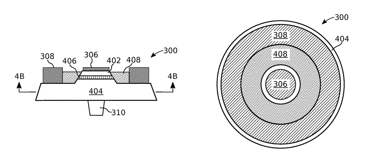
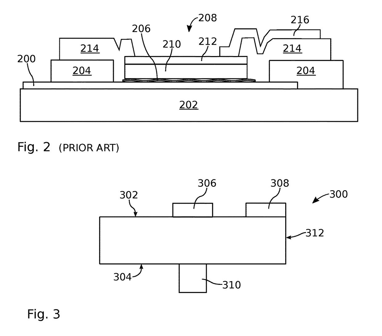
[0050]FIG. 3 is a partial cross-sectional view of a surface mount emissive element. The surface mount emissive element 300 comprises a top surface 302, a bottom surface 304, a first electrical contact 306 formed exclusively on the top surface, and a second electrical contact 308 formed exclusively on the top surface. By “exclusively on the top surface” it is meant that the electrical contacts or electrodes do not extend over the emissive element sides 312 or bottom surface 304. The electrical contacts may be a metal, doped semiconductor, or transparent conductive oxide (TCO) such as indium tin oxide (ITO). Although not explicitly shown as a distinct layer, the electrical contacts 306 and 308 may be solder or solder-coated (e.g., a eutectic solder) for subsequent connection to an emissive substrate. The emissive element 300 further comprises a post 310 extending from the bottom surface 304. In one aspect, the post 310 is centered in the middle of the bottom surface 304. One example o...


PUM


Abstract

A surface mount emissive element is provided with a top surface and a bottom surface. A first electrical contact is formed exclusively on the top surface, and a second electrical contact is formed exclusively on the top surface. A post extends from the bottom surface. An emissive display is also provided made from surface mount emissive elements and an emissions substrate. The emissions substrate has a top surface with a first plurality of wells formed in the emissions substrate top surface. Each well has a bottom surface, sidewalls, a first electrical interface formed on the bottom surface, and a second electrical interface formed on the bottom surface. The emissions substrate also includes a matrix of column and row conductive traces forming a first plurality of column / row intersections, where each column / row intersection is associated with a corresponding well. A first plurality of emissive elements populates the wells.

Description

RELATED APPLICATIONS[0001]Any and all applications, if any, for which a foreign or domestic priority claim is identified in the Application Data Sheet of the present application are hereby incorporated by reference under 37 CFR 1.57.BACKGROUND OF THE INVENTION[0002]1. Field of the Invention[0003]This invention generally relates to integrated circuits (ICs) and, more particularly, to a surface mount emissive element, and an emissive display made using the surface mount emissive elements.[0004]2. Description of the Related Art[0005]The current competing technologies for large area display are liquid crystal display (LCD), organic light emitting device (OLED) display, and more recently, inorganic LED display. The weaknesses of LCD, which the current disclosure directly addresses, are 1) low efficiency where only about 5% of the light generated by the backlight is seen as an image by the user, and 2) low dynamic range because the LC material cannot completely block light to produce a bl...

Claims


Application Information

Patent Timeline
Patent Type & Authority Patents(United States)
IPC IPC(8): H01L33/00H01L33/06H01L33/20H01L33/30H01L33/38H01L33/44H01L25/075H01L25/16H01L33/32H01L27/12
CPCH01L33/0079H01L25/0753H01L25/167H01L33/06H01L33/30H01L33/38H01L33/44H01L33/20H01L33/32H01L27/1214H01L33/62H01L2933/0066H01L33/0093
Inventor SCHUELE, PAUL J.SASAKI, KENJIULMER, KURTLEE, JONG-JAN
Owner ELUX INC
Why Eureka
Try Eureka