Supercharge Your Innovation With Domain-Expert AI Agents!

Lateral vias for connections to buried microconductors

a microconductors and via technology, applied in the field oflateral vias, can solve the problems of loss of device functionality, difficult handling, and extremely thin and fragile die of interes

Active Publication Date: 2018-05-15
NAT TECH & ENG SOLUTIONS OF SANDIA LLC
View PDF29 Cites 0 Cited by
  • Summary
  • Abstract
  • Description
  • Claims
  • Application Information

AI Technical Summary

Benefits of technology

The present invention relates to a component with a buried conductor that can be accessed through a lateral via. The lateral via is a microhole that provides access to the buried conductor and is connected to the component through a solder bump or a solder bump within a die stack. The invention also includes methods for forming the lateral via and the component with the lateral via. The technical effect of the invention is to provide a more efficient and reliable way to connect to buried conductors in components, which can improve performance and reliability.

Problems solved by technology

From a failure analysis perspective, 3-DI presents many challenges in order to access such electrical components, such as TSVs and solder bumps.
Alternatively, the die of interest can be extremely thin and fragile, which can be difficult to handle.
Many techniques involved with the preparation of 3-DI for failure analysis are destructive, in which a die has to be separated to access internal components, thereby resulting in loss of device functionality.
Accordingly, there is an emerging need for semi-destructive processes to access and to connect targeted TSVs and / or solder bumps on 3-DI components, such as those that are sandwiched between the stacked die and / or are not accessible from the large faces of the die stack.

Method used


Image

  • Lateral vias for connections to buried microconductors
  • Lateral vias for connections to buried microconductors
  • Lateral vias for connections to buried microconductors

Examples


example 1

[0113] Method and Apparatus for Making Electrical Connections to Buried Microscopic Conductors

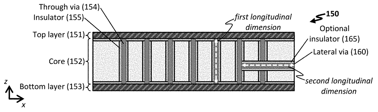
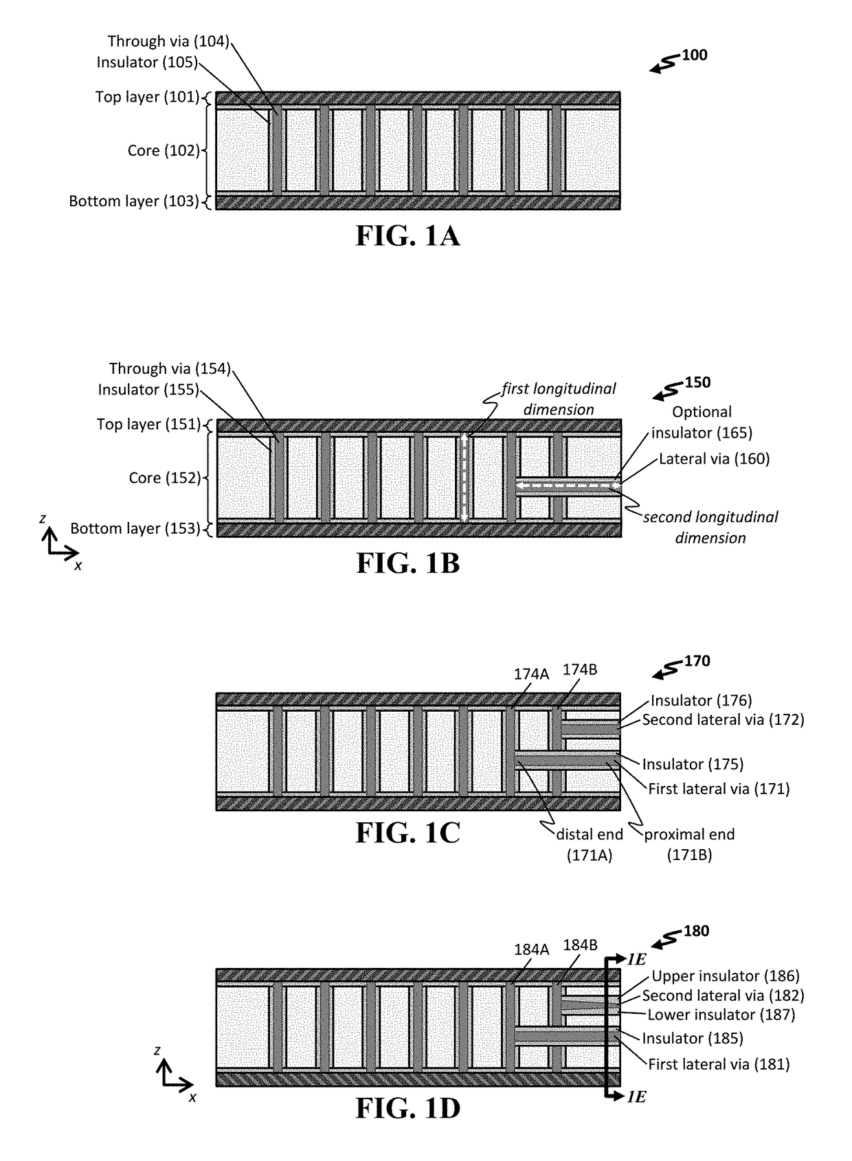
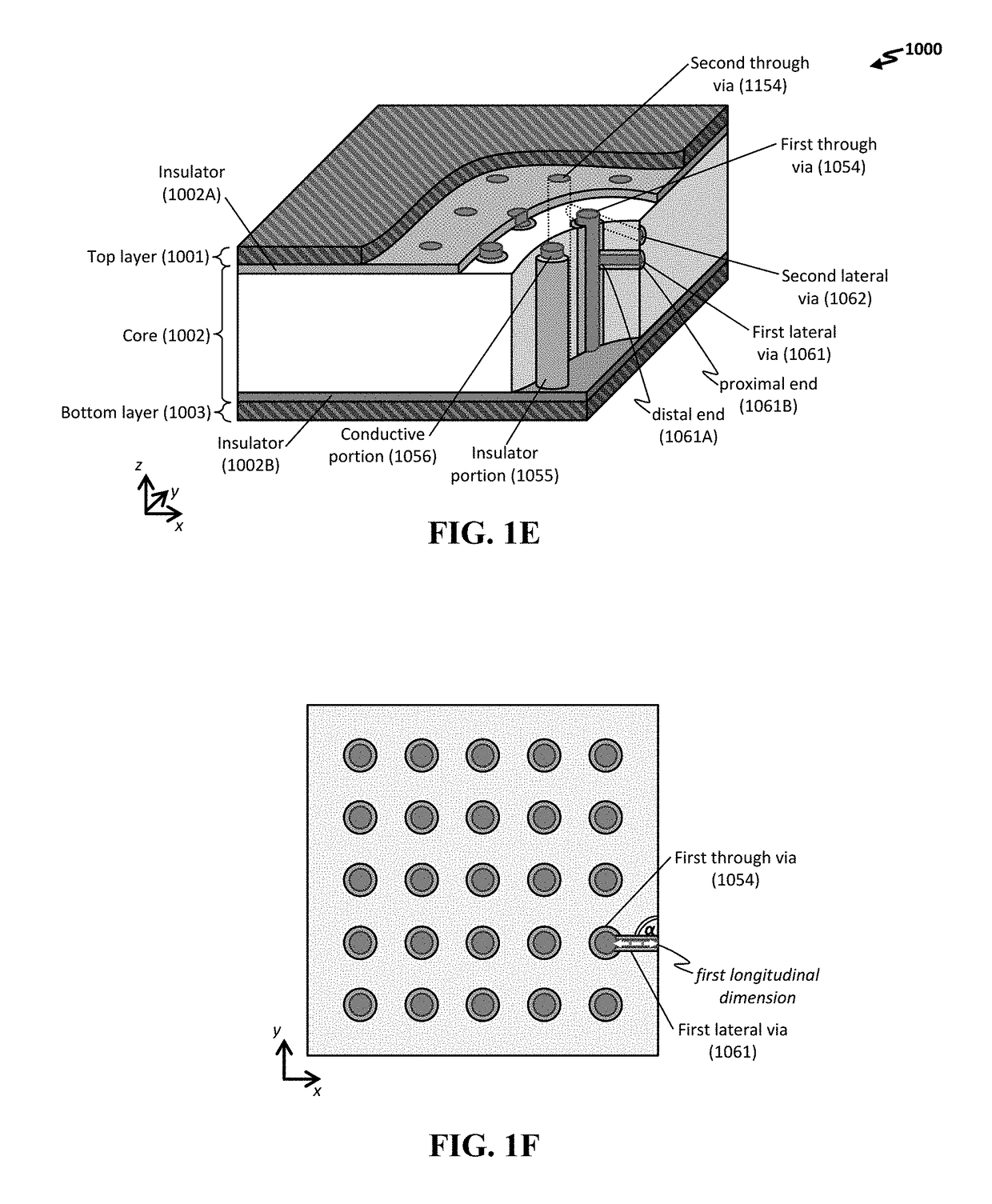
[0114]The present invention relates to methods and apparatuses including electrical connections to buried microconductors. Microconductors, which are buried at the start, could be metal trace conductors in a circuit board, through silicon vias, metal lines in integrated circuit, or wires under a protective underfill (e.g., composed of epoxy or a composite). Microholes can be formed to provide access to the buried microconductor, and then new metallic connections can be formed. Such metallic connections (e.g., lateral vias) can involve one or more metals deposited into created holes, which can be optionally preceded by insulator deposition on a sidewall of the hole in order to isolate the newly added metal from a semiconductor substrate (e.g., a semiconductor core).

[0115]An exemplary method can include a combination of subtractive and additive processes in order to build an electrical connec...


PUM


Abstract

The present invention relates to a lateral via to provide an electrical connection to a buried conductor. In one instance, the buried conductor is a through via that extends along a first dimension, and the lateral via extends along a second dimension that is generally orthogonal to the first dimension. In another instance, the second dimension is oblique to the first dimension. Components having such lateral vias, as well as methods for creating such lateral vias are described herein.

Description

STATEMENT OF GOVERNMENT INTEREST[0001]This invention was made with Government support under contract no. DE-AC04-94AL85000 awarded by the U.S. Department of Energy to Sandia Corporation. The Government has certain rights in the invention.FIELD OF THE INVENTION[0002]The present invention relates to a lateral via to provide an electrical connection to a buried conductor. In one instance, the buried conductor is a through via that extends along a first dimension, and the lateral via extends along a second dimension that is generally orthogonal to the first dimension. In another instance, the second dimension is oblique to the first dimension. Components having such lateral vias, as well as methods for creating such lateral vias are described herein.BACKGROUND OF THE INVENTION[0003]Stacked die for 3-dimensional integration (3-DI) are rapidly becoming a reality for commercial applications, including field-programmable gate arrays (FPGAs) and memory devices. Generally, 3-DI employs throug...

Claims


Application Information

Patent Timeline
Patent Type & Authority Patents(United States)
IPC IPC(8): H01L23/538H01L23/498H01L21/48H01L23/00H01L23/31
CPCH01L23/49827H01L23/49811H01L23/3178H01L23/49838H01L21/486H01L21/4853H01L21/4803H01L24/16H01L24/25H01L23/5384H01L23/5386H01L2224/16112H01L2224/165H01L2224/25105H01L23/3121H01L23/481H01L24/13H01L2224/13009H01L2224/13101H01L2224/16145H01L2224/16225H01L2924/15311H01L23/147H01L23/49822H01L25/0652H01L2225/06517H01L2225/06572H01L23/535H01L21/743H01L2924/014H01L2924/00014H01L21/76898H01L25/065
Inventor ADAMS, DAVID P.FISHGRAB, KIRA L.GRETH, KARL DOUGLASHENRY, MICHAEL DAVIDSTEVENS, JEFFREYHODGES, V. CARTERSHUL, RANDY J.GOEKE, RONALD S.GRUBBS, ROBERT K.
Owner NAT TECH & ENG SOLUTIONS OF SANDIA LLC
Features
  • R&D
  • Intellectual Property
  • Life Sciences
  • Materials
  • Tech Scout
  • Unparalleled Data Quality
  • Higher Quality Content
  • 60% Fewer Hallucinations
Learn More